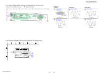
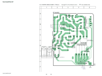
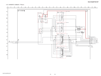
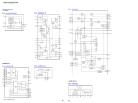
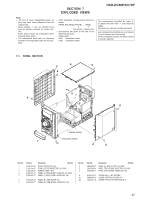
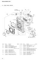
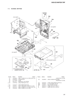
Sony HCD-EC68P Service Manual - Page 44
Pin No., Pin Name, Description
 |
View all Sony HCD-EC68P manuals
Add to My Manuals
Save this manual to your list of manuals |
Page 44 highlights
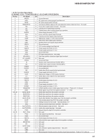
HCD-EC68P/EC78P Pin No. 61 62 63 64 65 66 67 68 69 70 71 72 73 74 75 76 77 78 79 80 81 82 83 84 85 86 87 88 89 90 91 92 93 94 95 96 97 98 99 100 Pin Name DOUT (PO6) AOUT (PO7) BCK (PO8) LRCK (PO9) AIN (PI4) BCKi (PI5) LRCKi (PI6) VDD1 VSS AWRC PVDD3 PDO TMAXS TMAX LPFN LPFo PVREF VCOF PVSS3 SLCo RFi RFRPi RFEQo VRo RESiN VMDiR TESTR AGCi RFo RVDD3 LDo MDi RVSS3 FNi2 (C) FNi1 (A) FPi2 (D) FPi1 (B) TPi (F) TNPC TNi (E) I/O Description O Digital audio data output terminal Not used O Audio data output terminal Not used O Bit clock signal output terminal Not used O L/R sampling clock signal output terminal Not used I Digital audio data input terminal Not used I Bit clock signal input terminal Not used I L/R sampling clock signal input terminal Not used - Power supply terminal (+1.5 V) - Ground terminal - Not used - Power supply terminal (+3.3 V) O Phase error margin signal between EFM signal and PLCK signal output terminal O TMAX detection signal output terminal Not used O TMAX detection signal output terminal I Inverted signal input from the operation amplifier for PLL loop filter O Signal output from the operation amplifier for PLL loop filter I Reference voltage (+1.65V) input terminal O VCO filter output terminal - Ground terminal O EFM slice level output terminal I RF signal input terminal I RF ripple signal input terminal O EFM slice level output terminal O Reference voltage (+1.65V) output terminal O External resistor connection terminal O Reference voltage (+1.65V) output terminal for automatic power control circuit O Low-pass filter terminal for RFEQO offset correction I RF signal amplitude adjustment amplification input terminal O RF signal generation amplification output terminal - Power supply terminal (+3.3 V) O Laser diode on/off control signal output to the automatic power control circuit "H": laser diode on I Light amount monitor input from the laser diode of optical pick-up block - Ground terminal I Main beam (C) input from the optical pick-up block I Main beam (A) input from the optical pick-up block I Main beam (D) input from the optical pick-up block I Main beam (B) input from the optical pick-up block I Sub beam (F) input from the optical pick-up block O External capacitor connection terminal I Sub beam (E) input from the optical pick-up block 44
-
 1
1 -
2
-
3
-
4
-
5
-
6
-
7
-
8
-
9
-
10
-
11
-
12
-
13
-
14
-
15
-
16
-
17
-
18
-
19
-
20
-
21
-
22
-
23
-
24
-
25
-
26
-
27
-
28
-
29
-
30
-
31
-
32
-
33
-
34
-
35
-
36
-
37
-
38
-
 39
39 -
 40
40 -
 41
41 -
 42
42 -
 43
43 -
 44
44 -
 45
45 -
 46
46 -
 47
47 -
 48
48 -
 49
49 -
50
-
51
-
52
-
53
-
54
-
55
-
56
-
57
-
58
-
59
-
60
-
61
-
62
-
63
-
64
-
65
-
66
 |
 |
