Sony HCD-EC68P Service Manual - Page 43
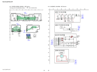
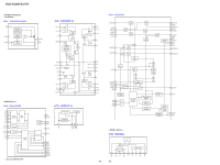
Cd Board, Ic101, Tc94a70fg-006 D, Hz Cd-mp3 Processor
 |
View all Sony HCD-EC68P manuals
Add to My Manuals
Save this manual to your list of manuals |
Page 43 highlights
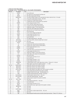
HCD-EC68P/EC78P • IC Pin Function Description CD BOARD IC101 TC94A70FG-006 (D, HZ (CD-MP3 PROCESSOR) Pin No. Pin Name I/O Description 1 AVSS3 - Ground terminal 2 RFZi I RF ripple zero crossing signal input terminal 3 RFRP O RF ripple signal output terminal 4 SBAD/RFDC O Sub beam addition signal or RF peak detection signal output terminal Not used 5 FEi O Focus error signal output terminal Not used 6 TEi O Tracking error signal output terminal 7 TEZi I Tracking error zero crossing signal input terminal 8 AVDD3 - Power supply terminal (+3.3 V) 9 FOo O Focus coil drive signal output terminal 10 TRo O Tracking coil drive signal output terminal 11 VREF I Reference voltage (+1.65V) input terminal 12 FMo O Sled motor drive signal output terminal 13 DMo O Spindle motor drive signal output terminal 14 VSSP3 - Ground terminal 15 VCOi I VCO control voltage input terminal 16 VDDP3 - Power supply terminal (+3.3 V) 17 VDD1 - Power supply terminal (+1.5 V) 18 VSS - Ground terminal 19 FGiN I FG signal input terminal Not used 20 IO0 (/HSO) I Disc inner position detection signal input terminal 21 IO1 (/UHSO) O Not used 22 XVSS3 - Ground terminal 23 XI I System clock input terminal (16.9344 MHz) 24 XO O System clock output terminal (16.9344 MHz) 25 XVDD3 - Power supply terminal (+3.3 V) 26 DVSS3 - Ground terminal 27 RO O Audio data (R-ch) output to the input selector 28 DVDD3 - Power supply terminal (+3.3 V) 29 DVR O Reference voltage (+1.65V) output terminal 30 LO O Audio data (L-ch) output to the input selector 31 DVSS3 - Ground terminal 32 VDDT3 - Power supply terminal (+3.3 V) 33 VSS1 - Ground terminal 34 VDD1 - Power supply terminal (+1.5 V) 35 VDDM1 - Power supply terminal (+1.5 V) 36 SRAMSTB I S-RAM standby mode control signal input terminal Fixed at "L" in this set 37 XRST I Reset signal input from the system controller "L": reset 38, 39 BUS0, BUS1 I Serial data input from the system controller 40 BUS2 (SO) I Serial data input from the system controller 41 BUS3 (SI) I Serial data input from the system controller 42 BUCK (CLK) I Serial data transfer clock signal input from the system controller 43 XCCE I Chip enable signal input from the system controller 44 TEST I Setting terminal for test mode Normally fixed at "L" 45 IRQ I Interrupt request signal input terminal Not used 46 AoUT3 (PO4) O Request signal output terminal Not used 47 AoUT2 (PO5) O Audio data output terminal Not used 48 PIO0 O Request signal output to the system controller 49, 50 PIO1, PIO2 O Not used 51 PIO3 I Gate signal input terminal Not used 52 VSS1 - Ground terminal 53 VDDT3 - Power supply terminal (+3.3 V) 54 SBSY O Subcode block sync signal output to the system controller 55 SBOK/FOK O Not used 56 IPF O Not used 57 SFSY/LOCK O Not used 58 ZDET O Zero detection signal output terminal Not used 59 GPIN I Not used 60 MS I Microcomputer interface mode selection signal input terminal Fixed at "H" in this set 43
-
 1
1 -
2
-
3
-
4
-
5
-
6
-
7
-
8
-
9
-
10
-
11
-
12
-
13
-
14
-
15
-
16
-
17
-
18
-
19
-
20
-
21
-
22
-
23
-
24
-
25
-
26
-
27
-
28
-
29
-
30
-
31
-
32
-
33
-
34
-
35
-
36
-
37
-
 38
38 -
 39
39 -
 40
40 -
 41
41 -
 42
42 -
 43
43 -
 44
44 -
 45
45 -
 46
46 -
 47
47 -
 48
48 -
49
-
50
-
51
-
52
-
53
-
54
-
55
-
56
-
57
-
58
-
59
-
60
-
61
-
62
-
63
-
64
-
65
-
66
 |
 |
