Sony PCV-J100 Reference Manual - Page 88
SDRAM RAS to CAS Delay, Memory Hole At 15M-16M
 |
View all Sony PCV-J100 manuals
Add to My Manuals
Save this manual to your list of manuals |
Page 88 highlights
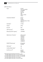
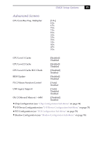
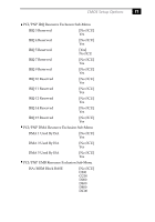
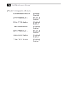
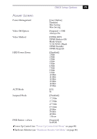
74 VAIO® Reference Manual Chip Configuration Sub-Menu SDRAM Configuration SDRAM CAS Latency SDRAM RAS to CAS Delay SDRAM RAS Precharge Time SDRAM Cycle Time (Tras, Trc) SDRAM Page Closing Policy CPU Latency Timer On-board VGA Display Cache Paging Mode Video Memory Cache Mode Memory Hole At 15M-16M PCI 2.1 Support High Priority PCI Mode Onboard PCI IDE Enable [By SPD] User Define 7ns (143MHz) 8ns (125MHz) [3T] [3T] [3T] [5T, 7T] 6T, 8T [All Banks] One Bank [Enabled] Disabled [Enabled] Disabled [Page open] Page close [UC] USWC [Disabled] Enabled [Enabled] Disabled [Enabled] Disabled [Both] Primary Secondary Disabled
-
 1
1 -
2
-
3
-
4
-
5
-
6
-
7
-
8
-
9
-
10
-
11
-
12
-
13
-
14
-
15
-
16
-
17
-
18
-
19
-
20
-
21
-
22
-
23
-
24
-
25
-
26
-
27
-
28
-
29
-
30
-
31
-
32
-
33
-
34
-
35
-
36
-
37
-
38
-
39
-
40
-
41
-
42
-
43
-
44
-
45
-
46
-
47
-
48
-
49
-
50
-
51
-
52
-
53
-
54
-
55
-
56
-
57
-
58
-
59
-
60
-
61
-
62
-
63
-
64
-
65
-
66
-
67
-
68
-
69
-
70
-
71
-
72
-
73
-
74
-
75
-
76
-
77
-
78
-
79
-
80
-
81
-
82
-
 83
83 -
 84
84 -
 85
85 -
 86
86 -
 87
87 -
 88
88 -
 89
89 -
 90
90 -
 91
91 -
 92
92 -
 93
93 -
94
-
95
-
96
-
97
-
98
-
99
-
100
-
101
-
102
-
103
-
104
-
105
-
106
-
107
-
108
-
109
-
110
-
111
-
112
-
113
-
114
 |
 |

VAIO
®
Reference Manual
74
Chip Configuration Sub-Menu
SDRAM Configuration
[By SPD]
User Define
7ns (143MHz)
8ns (125MHz)
SDRAM CAS Latency
[3T]
SDRAM RAS to CAS Delay
[3T]
SDRAM RAS Precharge Time
[3T]
SDRAM Cycle Time (Tras, Trc)
[5T, 7T]
6T, 8T
SDRAM Page Closing Policy
[All Banks]
One Bank
CPU Latency Timer
[Enabled]
Disabled
On-board VGA
[Enabled]
Disabled
Display Cache Paging Mode
[Page open]
Page close
Video Memory Cache Mode
[UC]
USWC
Memory Hole At 15M-16M
[Disabled]
Enabled
PCI 2.1 Support
[Enabled]
Disabled
High Priority PCI Mode
[Enabled]
Disabled
Onboard PCI IDE Enable
[Both]
Primary
Secondary
Disabled