EVGA 141-BL-E757-TR User Guide - Page 68
Award POST Codes, Description
 |
UPC - 843368010775
View all EVGA 141-BL-E757-TR manuals
Add to My Manuals
Save this manual to your list of manuals |
Page 68 highlights
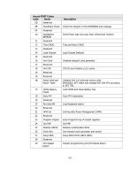
Award POST Codes Code Name 0D Reserved 0E CheckSum Check 0F Reserved 10 Autodetect EEPROM 11 Reserved 12 Test CMOS 13 Reserved 14 Load Chipset 15 Reserved 16 Init Clock 17 Reserved 18 Init CPU 19 Reserved 1A Reserved 1B Setup Interrupt Vector Table 1C CMOS Battery Check 1D Early PM 1E Reserved 1F Re-initial KB 20 Reserved 21 HPM init 22 Reserved 23 Program chipset 24 Init PNP 25 Shadow VBIOS 26 Clock Gen 27 Setup BDA 28 Reserved 29 CPU Speed detect Description Check the integrity of the ROM,BIOS and message Check Flash type and copy flash write/erase routines Test and Reset CMOS Load Chipset Defaults Initialize onboard clock generator CPU ID and initialize L1/L2 cache Initialize first 120 interrupt vectors with SPURIOUS_INT_HDLR and initialize INT 00h-1Fh according to INT_TBL Test CMOS and check Battery Fail Early PM initialization Load keyboard matrix Init Heuristic Power Management (HPM) Early Programming of chipset registers Init PNP Shadow system/video BIOS Init onboard clock generator and sensor Setup BIOS DATA AREA (BDA) Chipset programming and CPU Speed detect 68
-
 1
1 -
2
-
3
-
4
-
5
-
6
-
7
-
8
-
9
-
10
-
11
-
12
-
13
-
14
-
15
-
16
-
17
-
18
-
19
-
20
-
21
-
22
-
23
-
24
-
25
-
26
-
27
-
28
-
29
-
30
-
31
-
32
-
33
-
34
-
35
-
36
-
37
-
38
-
39
-
40
-
41
-
42
-
43
-
44
-
45
-
46
-
47
-
48
-
49
-
50
-
51
-
52
-
53
-
54
-
55
-
56
-
57
-
58
-
59
-
60
-
61
-
62
-
 63
63 -
 64
64 -
 65
65 -
 66
66 -
 67
67 -
 68
68 -
 69
69 -
 70
70 -
 71
71 -
 72
72 -
 73
73 -
74
-
75
-
76
 |
 |