Intel VC820 Design Guide - Page 139
DRCG Layout Example, 4.4 AGP Clock Routing Guidelines
 |
View all Intel VC820 manuals
Add to My Manuals
Save this manual to your list of manuals |
Page 139 highlights
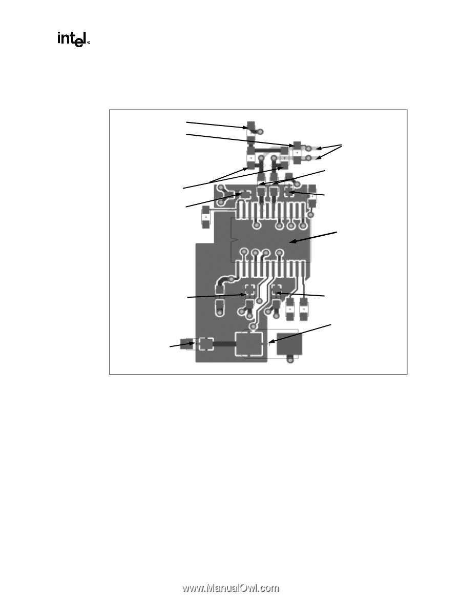
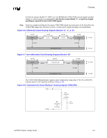
Clocking 4.3.1 DRCG Layout Example Figure 4-10. DRCG Layout Example Cmid - 100pF EMI Cap - 4pF Do Not Stuff Rp - 51 Ω (Keep trace from Rs to Rp short) Decoupling Cap - 0.1uF (Place VERY Near DRCG 3.3V Pin!) Decoupling Cap - 0.1uF (Place VERY Near DRCG 3.3V Pin!) Ferrite Bead (L22 in Reference Schematics) CTM/CTM# route on bottom layer Rs - 39 Ω (Keep trace from DRCG to Rs VERY short) Decoupling Cap - 0.1uF (Place VERY Near DRCG 3.3V Pin!) 3.3V-DRCG Flood Flood 3.3V-DRCG on the top layer around DRCG. Flood MUST include: 4 DRCG Power Pins 4 0.1uF Capacitors 1 10uF Bulk Capacitor 1 Isolation Ferrite Bead Decoupling Cap - 0.1uF (Place VERY Near DRCG 3.3V Pin!) Bulk Decoupling Cap - 10uF (Place Near DRCG) 4.4 4.5 AGP Clock Routing Guidelines The AGP clock must be routed with 20 mil spacing to all other signals and it must meet the length guidelines in Figure 4-2. Series Termination Resistors for CK133 Clock Outputs All used outputs require series termination resistors. The recommended resistor value will be defined by simulations. The stub length to the CK133 of these resistors can be compromised to make room for decoupling caps. The rule is to keep all resistor stubs within 250 mils of the CK133. If routing rules allow, Rpacks can be used if power dissipation is not exceeded for the Rpack. Intel®820 Chipset Design Guide 4-11
-
 1
1 -
2
-
3
-
4
-
5
-
6
-
7
-
8
-
9
-
10
-
11
-
12
-
13
-
14
-
15
-
16
-
17
-
18
-
19
-
20
-
21
-
22
-
23
-
24
-
25
-
26
-
27
-
28
-
29
-
30
-
31
-
32
-
33
-
34
-
35
-
36
-
37
-
38
-
39
-
40
-
41
-
42
-
43
-
44
-
45
-
46
-
47
-
48
-
49
-
50
-
51
-
52
-
53
-
54
-
55
-
56
-
57
-
58
-
59
-
60
-
61
-
62
-
63
-
64
-
65
-
66
-
67
-
68
-
69
-
70
-
71
-
72
-
73
-
74
-
75
-
76
-
77
-
78
-
79
-
80
-
81
-
82
-
83
-
84
-
85
-
86
-
87
-
88
-
89
-
90
-
91
-
92
-
93
-
94
-
95
-
96
-
97
-
98
-
99
-
100
-
101
-
102
-
103
-
104
-
105
-
106
-
107
-
108
-
109
-
110
-
111
-
112
-
113
-
114
-
115
-
116
-
117
-
118
-
119
-
120
-
121
-
122
-
123
-
124
-
125
-
126
-
127
-
128
-
129
-
130
-
131
-
132
-
133
-
 134
134 -
 135
135 -
 136
136 -
 137
137 -
 138
138 -
 139
139 -
 140
140 -
 141
141 -
 142
142 -
 143
143 -
 144
144 -
145
-
146
-
147
-
148
-
149
-
150
-
151
-
152
-
153
-
154
-
155
-
156
-
157
-
158
-
159
-
160
-
161
-
162
-
163
-
164
-
165
-
166
-
167
-
168
-
169
-
170
-
171
-
172
-
173
-
174
-
175
-
176
-
177
-
178
-
179
-
180
-
181
-
182
-
183
-
184
-
185
-
186
-
187
-
188
-
189
-
190
-
191
-
192
-
193
-
194
-
195
-
196
-
197
-
198
-
199
-
200
-
201
-
202
-
203
-
204
-
205
-
206
-
207
-
208
-
209
-
210
-
211
-
212
-
213
-
214
-
215
-
216
-
217
-
218
-
219
-
220
-
221
-
222
-
223
-
224
-
225
-
226
-
227
-
228
-
229
-
230
-
231
-
232
-
233
-
234
-
235
-
236
-
237
-
238
-
239
-
240
-
241
-
242
 |
 |