Intel VC820 Design Guide - Page 20
Platform Initiatives, 1.4.1 Direct Rambus*, 1.4.2 Streaming SIMD Extensions, 1.4.3 AGP 2.0
 |
View all Intel VC820 manuals
Add to My Manuals
Save this manual to your list of manuals |
Page 20 highlights
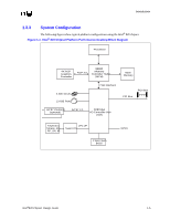
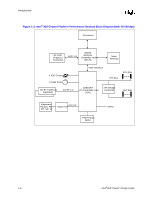
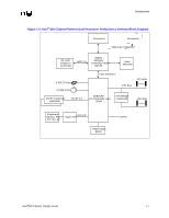
Introduction 1.4 1.4.1 1.4.2 1.4.3 1.4.4 Platform Initiatives Direct Rambus* The Direct Rambus* (RDRAM) initiative provides the memory bandwidth necessary to obtain optimal performance from the Pentium III processor as well as a high-performance AGP graphics controller. The MCH RDRAM interface supports 266 MHz, 300 MHz, 356 MHz, and 400 MHz operation; the latter delivers 1.6 GB/s of theoretical memory bandwidth; twice the memory bandwidth of 100 MHz SDRAM systems. Coupled with the greater bandwidth, the RDRAM protocol, which is heavily pipelined, provides substantially more efficient data transfer. The RDRAM memory interface can achieve greater than 95% utilization of the 1.6 GB/s theoretical maximum bandwidth. In addition to RDRAM's performance features, the new memory architecture provides enhanced power management capabilities. The powerdown mode of operation enables Intel® 820 chipset based systems to cost-effectively support suspend-to-RAM. Streaming SIMD Extensions The Pentium III processor provides 70 new Streaming SIMD (single instruction, multiple data) Extensions. The Pentium III new extensions are floating point SIMD extensions. Intel MMX™ technology provides integer SIMD extensions. The Pentium III processor new extensions complement the Intel MMX™ technology SIMD extensions and provide a performance boost to floating-point intensive 3D applications. AGP 2.0 The AGP 2.0 interface, along with Direct Rambus* memory technology, allows graphics controllers to access main memory at over 1 GB/s; twice the AGP bandwidth of previous AGP platforms. AGP 2.0 provides the infrastructure necessary for photorealistic 3D. In conjunction with Direct Rambus* and the Pentium III processor new Streaming SIMD Extensions, AGP 2.0 delivers the next level of 3D graphics performance. Hub Interface As I/O speeds increase, the demand placed on the PCI bus by the I/O bridge has become significant. With the addition of AC'97 and ATA/66, coupled with the existing USB, I/O requirements will begin to impact PCI bus performance. The Intel® 820 chipset's hub interface architecture ensures that the I/O subsystem, both PCI and the integrated I/O features (IDE, AC'97, USB, etc.), receives adequate bandwidth. By placing the I/O bridge on the hub interface instead of PCI, the hub architecture ensures that both the I/O functions integrated into the ICH and the PCI peripherals obtain the bandwidth necessary for peak performance. In addition, the hub interface's lower pin count allows a smaller package for the MCH and ICH. 1-8 Intel®820 Chipset Design Guide
-
 1
1 -
2
-
3
-
4
-
5
-
6
-
7
-
8
-
9
-
10
-
11
-
12
-
13
-
14
-
 15
15 -
 16
16 -
 17
17 -
 18
18 -
 19
19 -
 20
20 -
 21
21 -
 22
22 -
 23
23 -
 24
24 -
 25
25 -
26
-
27
-
28
-
29
-
30
-
31
-
32
-
33
-
34
-
35
-
36
-
37
-
38
-
39
-
40
-
41
-
42
-
43
-
44
-
45
-
46
-
47
-
48
-
49
-
50
-
51
-
52
-
53
-
54
-
55
-
56
-
57
-
58
-
59
-
60
-
61
-
62
-
63
-
64
-
65
-
66
-
67
-
68
-
69
-
70
-
71
-
72
-
73
-
74
-
75
-
76
-
77
-
78
-
79
-
80
-
81
-
82
-
83
-
84
-
85
-
86
-
87
-
88
-
89
-
90
-
91
-
92
-
93
-
94
-
95
-
96
-
97
-
98
-
99
-
100
-
101
-
102
-
103
-
104
-
105
-
106
-
107
-
108
-
109
-
110
-
111
-
112
-
113
-
114
-
115
-
116
-
117
-
118
-
119
-
120
-
121
-
122
-
123
-
124
-
125
-
126
-
127
-
128
-
129
-
130
-
131
-
132
-
133
-
134
-
135
-
136
-
137
-
138
-
139
-
140
-
141
-
142
-
143
-
144
-
145
-
146
-
147
-
148
-
149
-
150
-
151
-
152
-
153
-
154
-
155
-
156
-
157
-
158
-
159
-
160
-
161
-
162
-
163
-
164
-
165
-
166
-
167
-
168
-
169
-
170
-
171
-
172
-
173
-
174
-
175
-
176
-
177
-
178
-
179
-
180
-
181
-
182
-
183
-
184
-
185
-
186
-
187
-
188
-
189
-
190
-
191
-
192
-
193
-
194
-
195
-
196
-
197
-
198
-
199
-
200
-
201
-
202
-
203
-
204
-
205
-
206
-
207
-
208
-
209
-
210
-
211
-
212
-
213
-
214
-
215
-
216
-
217
-
218
-
219
-
220
-
221
-
222
-
223
-
224
-
225
-
226
-
227
-
228
-
229
-
230
-
231
-
232
-
233
-
234
-
235
-
236
-
237
-
238
-
239
-
240
-
241
-
242
 |
 |