Intel VC820 Design Guide - Page 40
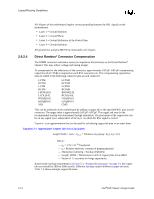
Direct Rambus* Connector Compensation, Equation 2-1. Approximate Copper Tab Area Calculation
 |
View all Intel VC820 manuals
Add to My Manuals
Save this manual to your list of manuals |
Page 40 highlights
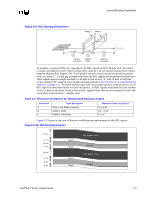
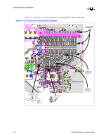
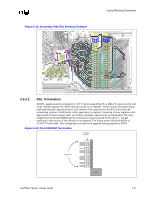
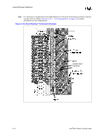
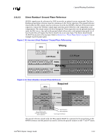
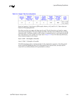
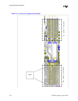
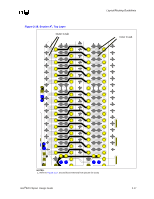
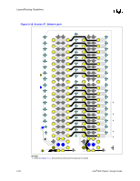
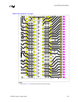
Layout/Routing Guidelines All 4 layers of the motherboard require correct grounding between the RSL signals on the motherboard: • Layer 1 = Ground Isolation • Layer 2 = Ground Plane • Layer 3 = Ground Reference in the Power Plane • Layer 4 = Ground Isolation All ground vias and pins MUST be connected to all 4 layers. 2.6.2.4 Direct Rambus* Connector Compensation The RIMM connector inductance causes an impedance discontinuity on the Direct Rambus* channel. This may reduce voltage and timing margin. To compensate for the inductance of the connector, approximately 0.65 pF-0.85 pF compensating capacitive tab (C-TAB) is required on each RSL connector pin. This compensating capacitance must be added to the following connector pins at each connector: LCTM RCTM LCFM RCFM LROW[2:0] LCOL[4:0] RDQA[8:0] RDQB[8:0] SCK LCTM# RCTM# LCFM# RCFM# RROW[2:0] RCOL[4:0] LDQA[8:0] LDQB[8:0] CMD This can be achieved on the motherboard by adding a copper tab to the specified RSL pins at each connector. The target value is approximately 0.65 pF-0.85 pF. The copper tab area for the recommended stackup was determined through simulation. The placement of the copper tabs can be on any signal layer, independent of the layer on which the RSL signal is routed. Equation is an approximation that can be used for calculating copper tab area on an outer layer. Equation 2-1. Approximate Copper Tab Area Calculation Length*Width = Area = Cplate * Thickness of prepreg / [(ε0) (εr) (1.1)] Where: - ε0 = 2.25 x 10⁻¹⁶ Farads/mil - εr = Relative dielectric constant of prepreg material - Thickness of prepreg = Stackup dependent - Length, Width = Dimensions in mils of copper plate to be added - Factor of 1.1 accounts for fringe capacitance. Based on the stackup requirement in Section 5.3, "Stackup Requirement" on page 5-1 the copper tab area should be 2800 to 3600 sq mils. Different stackups require different copper tab areas. Table 2-3 shows example copper tab areas. 2-14 Intel®820 Chipset Design Guide
-
 1
1 -
2
-
3
-
4
-
5
-
6
-
7
-
8
-
9
-
10
-
11
-
12
-
13
-
14
-
15
-
16
-
17
-
18
-
19
-
20
-
21
-
22
-
23
-
24
-
25
-
26
-
27
-
28
-
29
-
30
-
31
-
32
-
33
-
34
-
 35
35 -
 36
36 -
 37
37 -
 38
38 -
 39
39 -
 40
40 -
 41
41 -
 42
42 -
 43
43 -
 44
44 -
 45
45 -
46
-
47
-
48
-
49
-
50
-
51
-
52
-
53
-
54
-
55
-
56
-
57
-
58
-
59
-
60
-
61
-
62
-
63
-
64
-
65
-
66
-
67
-
68
-
69
-
70
-
71
-
72
-
73
-
74
-
75
-
76
-
77
-
78
-
79
-
80
-
81
-
82
-
83
-
84
-
85
-
86
-
87
-
88
-
89
-
90
-
91
-
92
-
93
-
94
-
95
-
96
-
97
-
98
-
99
-
100
-
101
-
102
-
103
-
104
-
105
-
106
-
107
-
108
-
109
-
110
-
111
-
112
-
113
-
114
-
115
-
116
-
117
-
118
-
119
-
120
-
121
-
122
-
123
-
124
-
125
-
126
-
127
-
128
-
129
-
130
-
131
-
132
-
133
-
134
-
135
-
136
-
137
-
138
-
139
-
140
-
141
-
142
-
143
-
144
-
145
-
146
-
147
-
148
-
149
-
150
-
151
-
152
-
153
-
154
-
155
-
156
-
157
-
158
-
159
-
160
-
161
-
162
-
163
-
164
-
165
-
166
-
167
-
168
-
169
-
170
-
171
-
172
-
173
-
174
-
175
-
176
-
177
-
178
-
179
-
180
-
181
-
182
-
183
-
184
-
185
-
186
-
187
-
188
-
189
-
190
-
191
-
192
-
193
-
194
-
195
-
196
-
197
-
198
-
199
-
200
-
201
-
202
-
203
-
204
-
205
-
206
-
207
-
208
-
209
-
210
-
211
-
212
-
213
-
214
-
215
-
216
-
217
-
218
-
219
-
220
-
221
-
222
-
223
-
224
-
225
-
226
-
227
-
228
-
229
-
230
-
231
-
232
-
233
-
234
-
235
-
236
-
237
-
238
-
239
-
240
-
241
-
242
 |
 |