Sony KLV32S400A Revision History - Page 25
Diagrams, Block Diagram, Circuit Board Location, Klv-26
 |
UPC - 011110668585
View all Sony KLV32S400A manuals
Add to My Manuals
Save this manual to your list of manuals |
Page 25 highlights
KLV-26,32,32/H/S,37 S400A RM-GA011 6-1. BLOCK DIAGRAM SECTION 6 DIAGRAMS Due to complexity of the board, performing component level field repairs are not recommended. Complete board replacement is required if service is necessary. 6-2. CIRCUIT BOARD LOCATION KLV-26,32,32/H/S,37 S400A BG1 Board Block Switch Panel GP Board (KLV-26,32,32/H/S S400A) Power Unit (G2D Board) (KLV-37S400A) HG4 Board (KLV-26,32,32/H/S S400A) HG4A Board (KLV-37S400A) - 24 -
-
 1
1 -
2
-
3
-
4
-
5
-
6
-
7
-
8
-
9
-
10
-
11
-
12
-
13
-
14
-
15
-
16
-
17
-
18
-
19
-
 20
20 -
 21
21 -
 22
22 -
 23
23 -
 24
24 -
 25
25 -
 26
26 -
 27
27 -
 28
28 -
 29
29 -
 30
30 -
31
-
32
-
33
-
34
-
35
-
36
-
37
-
38
-
39
-
40
-
41
-
42
-
43
-
44
-
45
-
46
-
47
-
48
-
49
-
50
-
51
-
52
-
53
-
54
-
55
-
56
-
57
-
58
-
59
-
60
-
61
-
62
-
63
-
64
-
65
-
66
-
67
-
68
-
69
-
70
-
71
-
72
-
73
-
74
-
75
-
76
-
77
-
78
-
79
-
80
-
81
 |
 |
– 24 –
KLV-26,32,32/H/S,37 S400A
RM-GA011
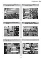
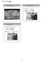
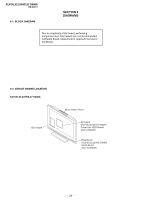
6-2. CIRCUIT BOARD LOCATION
KLV-26,32,32/H/S,37 S400A
Block Switch Panel
BG1 Board
GP Board
(KLV-26,32,32/H/S S400A)
Power Unit (G2D Board)
(KLV-37S400A)
HG4 Board
(KLV-26,32,32/H/S S400A)
HG4A Board
(KLV-37S400A)
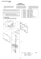
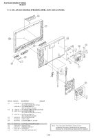
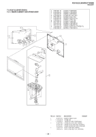
SECTION 6
DIAGRAMS
6-1. BLOCK DIAGRAM
Due to complexity of the board, performing
component level field repairs are not recommended.
Complete board replacement is required if service is
necessary.