AIWA CDC-X227 Service Manual - Page 28
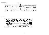
Description - how to set clock
 |
View all AIWA CDC-X227 manuals
Add to My Manuals
Save this manual to your list of manuals |
Page 28 highlights
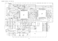
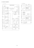
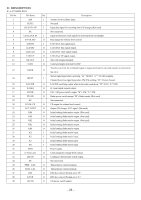
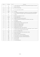
IC DESCRIPTION IC, LC72358N-9A71 Pin No. Pin Name I/O Description 1 XIN I System clock oscillator input. 2 TEST2 - Not used. 3 CD DATA IN I Input data signal for receiving from CD changer.(Not used) 4 NC - Not connected. 5 CD CLOCK IN I Input synchronous clock signal for receiving from CD changer. 6 E-VOL DO O Data output for volume level control. 7 LCD DI I LCD driver data signal input. 8 LCD DO O LCD driver data signal output. 9 LCD CLO O LCD driver clock signal output. 10 LCD CE O LCD driver CE signal output. 11 SQ OUT I Sub-code Q input terminal. 12 COIN O Command output terminal for DSP. Transfer-out clock for command output or output terminal for sub-code transfer-in clock from 13 CQCK O SQ OUT. Stereo signal input when receiving. "H"= MONO, "L"= ST FM reception. 14 SD/ST I Channel detection signal input when FM/AM seeking. "H"= Detect channel. 15 LOC/DX O LOC/DX switching output when in the radio seek mode. "H"= LOC, "L"= DX. 16 IF REQ O IF count signal request output. 17 BAND O FM / AM power switch output. "H"= AM, "L"= FM. 18 TU ON O Radio power switch output. "H"= Radio mode. (Not used) 19 NC - Not connected. 20 E-VOL CE O CE output for volume level control. 21 ACC-CONT O Output CD changer ACC signal. (Not used) 22 KS4 O Initial setting diode matrix output. (Not used) 23 KS3 O Initial setting diode matrix output. (Not used) 24 KS2 O Initial setting diode matrix output. (Not used) 25 KS1 O Initial setting diode matrix output. 26 KS0 O Initial setting diode matrix output. 27 K3 I Initial setting diode matrix input. 28 K2 I Initial setting diode matrix input. 29 K1 I Initial setting diode matrix input. 30 K0 I Initial setting diode matrix input. 31 VDD - Power supply. 32 E-VOL CLO O Clock output for volume level control. 33 LM SW O Loading or Thread Gain switch output. 34 NC - Not connected. 35 FEM+ LM+ O Thread motor control terminal. 36 FEM- LM- O Thread motor control terminal. 37 RW O RW disc control. Normal set to "H". 38 LP UP O RW disc control. Normal set to "L". 39 CD ON O CD power switch output. - 28 -
-
 1
1 -
2
-
3
-
4
-
5
-
6
-
7
-
8
-
9
-
10
-
11
-
12
-
13
-
14
-
15
-
16
-
17
-
18
-
19
-
20
-
21
-
22
-
 23
23 -
 24
24 -
 25
25 -
 26
26 -
 27
27 -
 28
28 -
 29
29 -
 30
30 -
 31
31 -
 32
32 -
 33
33 -
34
-
35
-
36
-
37
-
38
-
39
-
40
-
41
-
42
-
43
-
44
-
45
-
46
-
47
-
48
-
49
-
50
-
51
-
52
-
53
 |
 |
