AIWA CDC-X227 Service Manual - Page 34
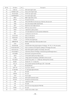
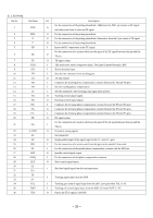
Pin No., Pin Name, Description, IC, LC75374E
 |
View all AIWA CDC-X227 manuals
Add to My Manuals
Save this manual to your list of manuals |
Page 34 highlights
IC, LC75374E Pin No. 1 2 Pin Name RVR IN R COM 3 ~ 5 RT1 ~ RT3 6 RT OUT 7 RS IN 8 NC 9 NC 10 RS3 11 RS OUT 12 FR IN 13 FR OUT 14 RR OUT 15 VSS 16 CL 17 DI 18 CE 19 VREF 20 RL OUT 21 FL OUT 22 FL IN 23 LS OUT 24 LS3 25 NC 26 NC 27 LS IN 28 LT OUT 29 ~ 31 LT3 ~ LT1 32 L COM 33 LVR IN 34 LSELO 35 AUX(L) 36 CHG(L) 37 TUN(L) 38 CD(L) 39 VDD 40 CD(R) I/O Description I 4dB volume control input. Must be driven at a low impedance. - 1dB volume control common pin. For the connection of capacitors that compensate for bass and treble in the tone control circuits. - A high-frequency compensation capacitors must be connected between T1 and T2. A low-frequency compensation capacitors must be connected between T2 and T3. O Tone control output. I Super bass input. Must be driven at a low impedance. - Connected to VSS. - Not connected. - For the connection of RCH super bass compensation capacitors. I Fader input. Must be driven at a low impedance. O Fader outputs. The front and rear sides can be attenuated independently. - Ground. I Serial data and clock input for control. Chip enable. Data is written in the internal latch when the chip enable signal goes "L" - from "H", and each analog switch is activated. Data transfer is enabled at "H". - Generates a 1/2VDD power source. A capacitor must be connected between VREF and VSS as a troubleshooting against power ripples. O Fader output. The front and rear sides can be attenuated independently. I Fader input. Must be driven at a low impedance. - For the connection of LCH super bass compensation capacitors. - Not connected. - Connected to VSS. I Super bass input. Must be driven at a low impedance. O Tone control output. For the connection of capacitors that compensate for bass and treble in the tone control circuit. - A high-frequency compensation capacitors must be connected between T1 and T2. A low-frequency compensation capacitors must be connected between T2 and T3. - 1dB volume control common pin. I 4dB volume control input. Must be driven at a low impedance. O Input selector output pin. I Signal input pins. - Not used. I Signal input pins. - Power supply. I Signal input pin. - 34 -
-
 1
1 -
2
-
3
-
4
-
5
-
6
-
7
-
8
-
9
-
10
-
11
-
12
-
13
-
14
-
15
-
16
-
17
-
18
-
19
-
20
-
21
-
22
-
23
-
24
-
25
-
26
-
27
-
28
-
 29
29 -
 30
30 -
 31
31 -
 32
32 -
 33
33 -
 34
34 -
 35
35 -
 36
36 -
 37
37 -
 38
38 -
 39
39 -
40
-
41
-
42
-
43
-
44
-
45
-
46
-
47
-
48
-
49
-
50
-
51
-
52
-
53
 |
 |
