AIWA CDC-X227 Service Manual - Page 30
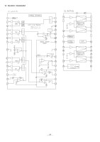
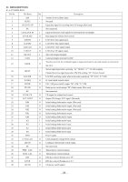
IC, LA9241ML
 |
View all AIWA CDC-X227 manuals
Add to My Manuals
Save this manual to your list of manuals |
Page 30 highlights
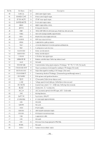
IC, LA9241ML Pin No. Pin Name 1 FIN2 2 FIN1 3 E 4 F 5 TB 6 TE- 7 TE 8 TESI 9 SCI 10 TH 11 TA 12 TD- 13 TD 14 JP 15 TO 16 FD 17 FD- 18 FA 19 FA- 20 FE 21 FE- 22 A-GND 23 NC 24 SP 25 SPG 26 SP- 27 SPD 28 SLEQ 29 SLD 30 SL- 31 SL+ 32 JP- 33 JP+ 34 TGL 35 TOFF 36 TES I/O Description For the connection of the pickup photodiode. Addition to the FIN1 pin creates an RF signal O and subtraction from it create an EF signal. O For the connection of the pickup photodiode. O For the connection of the pickup photodiode. Subtraction from the F pin creates a TE signal. O For the connection of the pickup photodiode. I Inputs the DC components in the TE signal. For the connection of a resistor which sets the gain of the TE signal between this pin and the O TE pin. O TE signal output. I TES (track error sense) comparator input. The signal is passed through a BPF. I Shock detection input. I Sets the time constant for the tracking gain. O TA amp output. I Composes the tracking phase compensation constant between the TD and VR pins. I Sets the tracking phase compensation. I Sets the amplitude of the tracking jump signal (kick pulses). O Tracking control signal output. O Focusing control signal output. I Composes the focusing phase compensation constant between the FD and FA pins. O Composes the focusing phase compensation constant between the FD and FA pins. I Composes the focusing phase compensation constant between the FD and FA pins. O FE signal output. For the connection of a resistor which sets the gain of the FE signal between this pin and the I TE pin. O Ground of analog signals. - Not connected. O Single-ended output of the signal input to the CV+ and CV- pins. I For the connection of a resistor which sets the gain in the spindle 12cm mode. I For the connection of the spindle phase compensation constant with the SPD pin. O Spindle control signal output. I For the connection of sled phase compensation constant. O Sled control signal output. I Sled feed signal input from the microprocessor. I Tracking signal input from the DSP. I Tracking gain control signal input from the DSP. Low gain when TGL is "H". I Tracking off control signal input from the DSP. Off when TOFF is "H". O Output the TES signal to the DSP. - 30 -
-
 1
1 -
2
-
3
-
4
-
5
-
6
-
7
-
8
-
9
-
10
-
11
-
12
-
13
-
14
-
15
-
16
-
17
-
18
-
19
-
20
-
21
-
22
-
23
-
24
-
 25
25 -
 26
26 -
 27
27 -
 28
28 -
 29
29 -
 30
30 -
 31
31 -
 32
32 -
 33
33 -
 34
34 -
 35
35 -
36
-
37
-
38
-
39
-
40
-
41
-
42
-
43
-
44
-
45
-
46
-
47
-
48
-
49
-
50
-
51
-
52
-
53
 |
 |
