AIWA CDC-X227 Service Manual - Page 33
AIWA CDC-X227 Manual
 |
View all AIWA CDC-X227 manuals
Add to My Manuals
Save this manual to your list of manuals |
Page 33 highlights
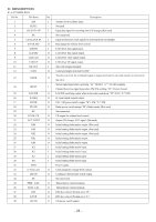
Pin No. 42 43 44 45 46 47 48 49 50 51 52 53 54 55 56 57 58 59 60 61 62 63 64 Pin Name RMUTE XVDD XOUT XIN XVSS SBSY EFLG PW SFSY SBCK FSX WRQ RWC SQOUT COIN CQCK RES TST11 16M 4.2M TEST5 CS TEST1 I/O Description O Right channel mute output. (Not used) - Crystal oscillator power supply. O Connection for a 16.93 MHz crystal oscillator element. I - Crystal oscillator ground. (Must be connected to 0V.) O Subcode clock synchronization signal output. (Not used) O C1, C2, sigle an double error correction monitor. (Not used) O Subcode P, Q, R, S, T, U and W output. (Not used) Subcode frame synchronization signal output. This signal falls when the subcode are in standby O state. (Not used) I Subcode read out clock input. This is a Schmitt input. (Must be connected to 0 V.) O Output pin for the 7.35 kHZ synchronization signal divided from the crystal oscillator. (Not used) O Subcode Q output standby output. I Read/write control input. This is a Schmitt input. O Subcode Q output. I Command input pin from control microprocessor. Input for both the command input acquisition clock and the SQOUT pin subcode I readout clock input pin. This is Schmitt input. I Reset input. This pin must be set low briefly after power is first applied. O Test output. Leave open. (Normally output a low level.) (Not used.) O 16.9344 MHz output. (Not used.) O 4.2336 MHz output. I Test input. A pull-down resistor is built-in. (Must be connected to 0V.) Chip select input. A pull-down resistor is built-in. I (Must be connected to 0 V.) I Test input. No pull-down resistor. (Must be connected to 0V.) - 33 -
-
 1
1 -
2
-
3
-
4
-
5
-
6
-
7
-
8
-
9
-
10
-
11
-
12
-
13
-
14
-
15
-
16
-
17
-
18
-
19
-
20
-
21
-
22
-
23
-
24
-
25
-
26
-
27
-
 28
28 -
 29
29 -
 30
30 -
 31
31 -
 32
32 -
 33
33 -
 34
34 -
 35
35 -
 36
36 -
 37
37 -
 38
38 -
39
-
40
-
41
-
42
-
43
-
44
-
45
-
46
-
47
-
48
-
49
-
50
-
51
-
52
-
53
 |
 |
