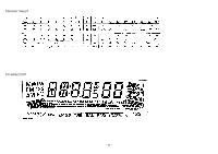
AIWA CDC-X227 Service Manual - Page 31
AIWA CDC-X227 Manual
 |
View all AIWA CDC-X227 manuals
Add to My Manuals
Save this manual to your list of manuals |
Page 31 highlights
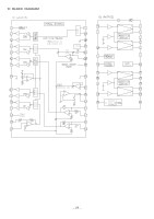
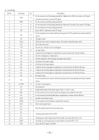
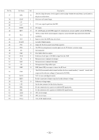
Pin No. 37 38 39 40 41 42 43 44 45 46 47 48 49 50 51 52 53 54 55 56 57 58 59 60 61 62 63 64 Pin Name HFL SLOF CVCV+ RFSM RFS- SLC SLI D-GND FSC TBC NC DEF CLK CL DAT CE DRF FSS VCC2 REFI VR LF2 PH1 BH1 LDD LDS VCC1 I/O Description The HFL (high frequency level) signal is used to judge whether the main beam is positioned on O the pit or on the mirror. I Sled servo off control input. I CLV error signal input from the DSP. O RF output. O Set the RF gain and the EFM singal's 3T compensation constant together with the RFSM pin. The SLC (slice level control) signal is output to control the DSP's data slice level of the RF O waveform. I Input to control the DSP's data slice level. - Ground of digital signals. O Output for the focus search smoothing capacitor. I The TBC (tracking balance control) signal sets the EF balance variation range. - Not connected. O Disc defect detection output. I Reference clock input. 4.23 MHz is input from the DSP. I Microprocessor command clock input. I Microprocessor command data input. I Microprocessor chip enable input. O DRF (detect RF) is an output to detect the RF level. The FSS (focus search select) signal switches the focus search modes (+/-search / +search with I respect to the reference voltage). (Connected to D-GND) - VCC of servo and digital circuits. - For the connection of bypass capacitor for the reference voltage. O Reference voltage output. - Set the time constant for disc defect detection. - For the connection of a capacitor to hold the RF signal peak. - For the connection of a capacitor to hold the RF signal bottom. O APC circuit output. I APC circuit input. - VCC of RF signal circuits. - 31 -
-
 1
1 -
2
-
3
-
4
-
5
-
6
-
7
-
8
-
9
-
10
-
11
-
12
-
13
-
14
-
15
-
16
-
17
-
18
-
19
-
20
-
21
-
22
-
23
-
24
-
25
-
 26
26 -
 27
27 -
 28
28 -
 29
29 -
 30
30 -
 31
31 -
 32
32 -
 33
33 -
 34
34 -
 35
35 -
 36
36 -
37
-
38
-
39
-
40
-
41
-
42
-
43
-
44
-
45
-
46
-
47
-
48
-
49
-
50
-
51
-
52
-
53
 |
 |
