Epson LQ 1050 Technical Manual - Page 203
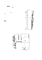
REV.-A, MM1/O, DB7-O, IN7-O
 |
View all Epson LQ 1050 manuals
Add to My Manuals
Save this manual to your list of manuals |
Page 203 highlights
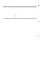
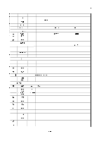
REV.-A This gate array is accessed by READing and WRITEing the memory mapped 1/0 addresses (MM IO) using the internal address decoder. The MMIO Ports for this gate array are OOH to 07H, accessed by the lower three bits (AO to A2) of the address bus. Table A-1 O shows the operation of the memory mapped 1/0 addresses. Table A-10. GA E05A16GA Control Functions MM1/O Address OOH 01 H 02H 03H 04H READ/ WRITE READ WRITE READ WRITE READ WRITE READ WRITE READ WRITE Control Functions PA7-O + DB7-O (Read) The data is inverted. DB7-O + PB7-O (Write) The data is inverted. IN7-O + DB7-O (Read) The data is inverted. DB7-O ~ PC7-O (Write) The data is inverted except bit O and 1. Read hard-ware BUSY signal (DBO) When DBO is high, parallel data is latched in gate array. Write interface parameter to interface control port. Bit 7: Print data O: "1" bit is print data; 1: "O" bit is print data. Bit 6: Acknowledge signal O: inactive state 1: active state Bit 5: Busy signal O: High level is active state. 1: Low level is active state. Bit 4: Software Busy signal O: Software Busy state. 1: Ready state. Bit 3: ERR signal O: inactive state. 1: active state. Bit 2: PE signal O: inactive state. 1: active state. Bit 1: Serial data input selection. O: IN7. 1 : RX DIN. Bit O: Parallel data latch timing. O: Rising edge of STRB. 1: Falling edge of STRB. Read the converted Italic CG data. The data is shifted at the falling edge of the RD signal. Shift out the MS bit of the 24 bits shift register. MSB24 ~ DB7 The data is shifted at the rising edge fo RD signal. Load shift register. 1st: DB7-O ~ Bit 23-16 2nd: DB7-O ~ Bit 15-8 3rd: DB7-O ~ Bit 7-O A-1 7
-
 1
1 -
2
-
3
-
4
-
5
-
6
-
7
-
8
-
9
-
10
-
11
-
12
-
13
-
14
-
15
-
16
-
17
-
18
-
19
-
20
-
21
-
22
-
23
-
24
-
25
-
26
-
27
-
28
-
29
-
30
-
31
-
32
-
33
-
34
-
35
-
36
-
37
-
38
-
39
-
40
-
41
-
42
-
43
-
44
-
45
-
46
-
47
-
48
-
49
-
50
-
51
-
52
-
53
-
54
-
55
-
56
-
57
-
58
-
59
-
60
-
61
-
62
-
63
-
64
-
65
-
66
-
67
-
68
-
69
-
70
-
71
-
72
-
73
-
74
-
75
-
76
-
77
-
78
-
79
-
80
-
81
-
82
-
83
-
84
-
85
-
86
-
87
-
88
-
89
-
90
-
91
-
92
-
93
-
94
-
95
-
96
-
97
-
98
-
99
-
100
-
101
-
102
-
103
-
104
-
105
-
106
-
107
-
108
-
109
-
110
-
111
-
112
-
113
-
114
-
115
-
116
-
117
-
118
-
119
-
120
-
121
-
122
-
123
-
124
-
125
-
126
-
127
-
128
-
129
-
130
-
131
-
132
-
133
-
134
-
135
-
136
-
137
-
138
-
139
-
140
-
141
-
142
-
143
-
144
-
145
-
146
-
147
-
148
-
149
-
150
-
151
-
152
-
153
-
154
-
155
-
156
-
157
-
158
-
159
-
160
-
161
-
162
-
163
-
164
-
165
-
166
-
167
-
168
-
169
-
170
-
171
-
172
-
173
-
174
-
175
-
176
-
177
-
178
-
179
-
180
-
181
-
182
-
183
-
184
-
185
-
186
-
187
-
188
-
189
-
190
-
191
-
192
-
193
-
194
-
195
-
196
-
197
-
 198
198 -
 199
199 -
 200
200 -
 201
201 -
 202
202 -
 203
203 -
 204
204 -
 205
205 -
 206
206 -
 207
207 -
 208
208 -
209
-
210
-
211
-
212
-
213
-
214
-
215
-
216
-
217
-
218
-
219
-
220
-
221
-
222
-
223
-
224
-
225
 |
 |
