Garmin GAD 42 Maintenance Manual - Page 10
CPU Circuitry, FPGA Devices, Serial EEPROM, ARINC 429 Receivers
 |
View all Garmin GAD 42 manuals
Add to My Manuals
Save this manual to your list of manuals |
Page 10 highlights
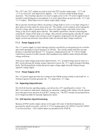
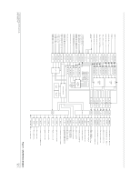
7.12 CPU Circuitry The GAD 42 CPU board contains the CPU which is clocked at 32 MHz and then internally divided to 16 MHz. This 16 MHz clock output is present anytime power is applied to the GAD 42, and is used to clock the two FPGA IC's. A low power micromonitor watchdog holds the CPU in reset if Vcc is too low, and if the micromonitor latched output fails to toggle indicating CPU lockup. Three IC address latches latch CPU address data when present on the shared address/data lines so they can then pass data. A flash memory device contains unit software code, and can be erased and re-programmed by RS-232 interface when the GAD 42 is in test mode. The VPP program voltage for this device is provided by an 11.8 VDC regulator. A Static Ram device provides storage capacity while the CPU is in operation. DISCRETE INPUTS to the CPU are read through two line driver IC's, and DISCRETE OUTPUTS from the CPU are latched for output by two D flip-flop IC's. CPU serial I/O is level-shifted by an RS-422 I/O level shifter for RS-422 format input and output, and by an RS-232 I/O level shifter for RS-232 format input and output. After level shifting, both RS-232 and RS-422 I/O are received and transmit directly from internal serial I/O within the CPU. 7.13 FPGA Devices The CPU board contains two FPGA devices which have access to the CPU address/data bus through two bus transceivers. These devices contain state machine logic that is configured on unit power-up by programming code contained in flash memory. Both FPGA's are programmed by serial data. If the devices are programmed and operating properly, they will both provide a 12 kHz clock signal at the 12 kHz output of each device. One of the FPGAs (FPGA1) contains the GPS ARINC 429 and NAV ARINC 429 serial data receivers, and the ARINC 561/568 and King serial data transmitters. The other FPGA (FPGA2) contains the HDG ARINC 429 and RG ARINC 429 serial data receivers, and the LO-SPD ARINC 429 and HI-SPD ARINC 429 serial data receivers. 7.14 Serial EEPROM Configuration and calibration data is stored in a serial EEPROM IC on the CPU board. The serial data bus to the EEPROM is shared with the DC A/D converter described previously. 7.15 ARINC 429 Receivers The GPS, NAV, Heading, and Radar Graphics ARINC 429 receivers are all input to identical level shifters on the CPU board. The differential A and B inputs have overvoltage protection provided by two diodes and two resistors. If A is low, and B is high, current flows through two resistors, turning on a NPN transistor which then turns on a PNP output transistor. This causes Vcc to be applied across a resistor, and out the the FPGA "A" input. If B is low, and A is high, current flows in the opposite direction through two resistors, turning on a different NPN transistor which then turns on a different PNP output transistor. This causes Vcc to be applied across a resistor, and out to FPGA "B" input. GAD 42 MAINTENANCE MANUAL P/N 190-00159-01 Page 9 Rev. A
-
 1
1 -
2
-
3
-
4
-
 5
5 -
 6
6 -
 7
7 -
 8
8 -
 9
9 -
 10
10 -
 11
11 -
 12
12 -
 13
13 -
 14
14
 |
 |