Garmin GAD 42 Maintenance Manual - Page 12
Valid High Inputs, Control Outputs, ASSEMBLY DRAWING
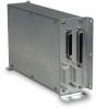 |
View all Garmin GAD 42 manuals
Add to My Manuals
Save this manual to your list of manuals |
Page 12 highlights
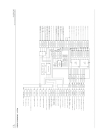
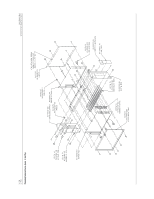
7.20 Valid High Inputs All valid high inputs are located on the CPU board, and are identical to the HDG VALID HI input described here. When the HDG_VALID_HI input pin is connected to aircraft power voltage over 10 V, a diode conducts base current to a transistor through a resistor. This turns on the transistor, and the output normally connected to Vcc through a resistor is shorted to ground. When this output is grounded, and the corresponding valid low output is active (high), a logic high is generated by a digital IC. The CPU reads this as a logic high from the data bus through a discrete input latch. When the HDG_VALID_HI input is open, grounded, or connected to a voltage less than 10 V, no base current can flow, and the transistor is turned off. This results in a logic low being read by the CPU. A diode provides transient voltage protection for the transistor. A capacitor and resistor form a low-pass filter to reduce high-frequency noise at the input. 7.21 Control Outputs All control outputs are located on the CPU board, and are identical to the output described here. When the DIST_IND_OUT latch output from the CPU data bus is at logic high, gate voltage is applied through a resistor to a power FET. This turns the FET on, and DIST_IND_CONTROL is grounded through a resistor. If the current through the resistor exceeds about 0.5 A, enough voltage is developed across a second resistor to turn on Q581. This shorts the gate voltage applied to the FET to ground, turning it off for over-current protection. A zener provides transient protection for the FET. 8.0 ASSEMBLY DRAWING Figure 2, page 13, shows an assembly drawing (with part numbers) for the GAD 42. GAD 42 MAINTENANCE MANUAL P/N 190-00159-01 Page 11 Rev. A
-
 1
1 -
2
-
3
-
4
-
5
-
6
-
 7
7 -
 8
8 -
 9
9 -
 10
10 -
 11
11 -
 12
12 -
 13
13 -
 14
14
 |
 |