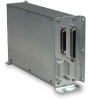
Garmin GAD 42 Maintenance Manual - Page 11
ARINC 429 Transmitters, ARINC 561/568 Transmitters, King Serial Transmitters, Discrete Inputs
 |
View all Garmin GAD 42 manuals
Add to My Manuals
Save this manual to your list of manuals |
Page 11 highlights
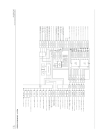
7.16 ARINC 429 Transmitters The GPS Lo-Speed and Hi-speed ARINC 429 transmitters are output from the FPGA to identical level shifters and output drivers on the CPU board. During the time between data bits, the FPGA output is tri-stated. During this time, the output data stream from the FPGA is biased to 2.5 V by two resistors. During transmission of data bits, the FPGA data output is either 0 or 4.75 V, which takes authority over the bias resistors. A unity-gain buffer which applies the signal to an op amp where it is inverted and level-shifted such that the output varies +/- 5 V from ground. The transition edges are rounded by in order to meet ARINC 429 specifications. From here, the signal is routed to both a non-inverting and an inverting output amp. The output amps consist of op-amps which drive push-pull transistor pairs that are within their feedback loops. Feedback resistors set the gain, and high-frequency attenuation is provided by capacitors and resistors for the non-inverting output amp, and by a different set of capacitors and resistors for the inverting output amp. Transient protection for the output amps is provided by zener diodes. 7.17 ARINC 561/568 Transmitters The ARINC 561/568 clock, data, sync, and continuous clock outputs are output from the FPGA to identical output drivers on the CPU board. The FPGA output is applied to a low-pass filter to round the transition edges, and then to the output amp. The output amp consists of an op-amp, which drives a push-pull transistor pair that are within the feedback loop. Feedback resistors set the gain at 2.2, and high-frequency attenuation is provided by an RC network. Transient protection for the output amp is provided by a zener diode. 7.18 King Serial Transmitters The King serial data and clock transmitters are identical to the ARINC 561/568 transmitters described previously with two exceptions: Gain is set at 1.8 rather than 2.2, and the output is diode-isolated from the bus such that only a high output can be transmitted onto the bus. King serial data transmission is initiated by a King serial request (KING_SERIAL_RQST) input going to logic low. 7.19 Discrete Inputs All discrete inputs are located on the CPU board, and are identical to the TEST input described here. When the TEST input pin is grounded through a resistance from zero to 100 ȍ, base current through a digital transistor flows through a resistor turning it on. When the transistor turns on, Vcc is applied across another resistor and read as a logic high from the data bus by the CPU through either a discrete input latch or an FPGA input latch. When the TEST input is open or connected to aircraft power voltage, no base current can flow, and the digital transistor is turned off. This results in a logic low being read by the CPU. A diode provides transient voltage protection for the transistor. A capacitor and resistor form a low-pass filter to reduce highfrequency noise at the input. GAD 42 MAINTENANCE MANUAL P/N 190-00159-01 Page 10 Rev. A
-
 1
1 -
2
-
3
-
4
-
5
-
 6
6 -
 7
7 -
 8
8 -
 9
9 -
 10
10 -
 11
11 -
 12
12 -
 13
13 -
 14
14
 |
 |