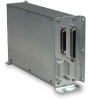
Garmin GAD 42 Maintenance Manual - Page 8
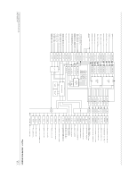
Filter/Attenuator, Synchronous Rectifier, VAC Reference Inputs, Synchro Analog-to-Digital Converter - system
 |
View all Garmin GAD 42 manuals
Add to My Manuals
Save this manual to your list of manuals |
Page 8 highlights
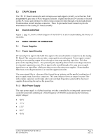
7.4 Filter/Attenuator As can be seen from the block diagram, the synchro heading inputs HEADING X and HEADING Y are first applied to a filter and attenuator network where they are attenuated and filtered by an RC circuit. A dual switching diode clamps over-voltage inputs at +5 V and -5 V which are the maximum input voltage to be applied to CMOS analog switches. An 11.8 Vac (16.7 V peak) synchro input at HEADING X or HEADING Y is attenuated by a filter/attenuator network to 2.5 Vac (3.57 V peak). 7.5 Synchronous Rectifier The HEADING X and HEADING Y inputs are buffered to a lower impedance before being applied to a synchronous rectifier CMOS switch. The outputs of the CMOS switch are then applied to an RC circuit to reduce any switching noise, and limit rate of change. A DC amplifier provides gain so that the DC voltage range matches the input voltage range of the analog-todigital converter. The DC amplifier outputs are sent directly to the CPU PC Board where they are read by the A/D converter. 7.6 26 VAC Reference Inputs Because all 26 Vac reference inputs (shown in the lower left corner of the block diagram) are processed by identical circuitry, only the 26 Vac indicator reference input is discussed here. The differential indicator reference voltages are first input to an RC filter network where they are filtered, clamped, and then applied to a differential amplifier. The differential amplifier attenuates the reference-input signals. The attenuator output is applied to two circuits. First is a buffer amplifier: its output is used to monitor the AC reference input amplitude, and also is used as the reference voltage (VREF) for the D/A converters described later. The amplitude of VREF is determined by synchronously rectifying the input in the CMOS analog switch as previously described for HEADING X and HEADING Y inputs. The output of the synchronous rectifier is then filtered by an RC network and buffered by an op amp. The output of the buffer is then read by an 8-bit serial 10-channel DC A/D converter on the CPU PC Board. All other 26 Vac reference inputs are processed the same way on the Analog PC Board, and read by the same A/D converter on the CPU PC Board. The second circuit that the attenuator output is applied to derives the signal that is applied to the control input of the CMOS analog switch. The first network of this circuit is a -90 Degree Phase Shift. The output is then applied to a zero crossing detector. The output of this circuit is a 400 Hz square wave delayed by 90 degrees from the input voltage. A pulse generator circuit generates a pulse at every rising edge of the square wave applied to it. The pulse generator drives the control input of the CMOS analog switch. 7.7 Synchro Analog-to-Digital Converter All synchro inputs are converted to DC on the analog PC board as previously described above for HEADING X and HEADING Y, and applied to one of two 4 channel, 12-bit A/D converters on the CPU PC Board. GAD 42 MAINTENANCE MANUAL P/N 190-00159-01 Page 7 Rev. A
-
 1
1 -
2
-
 3
3 -
 4
4 -
 5
5 -
 6
6 -
 7
7 -
 8
8 -
 9
9 -
 10
10 -
 11
11 -
 12
12 -
 13
13 -
14
 |
 |