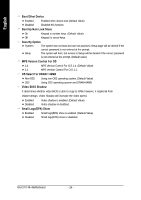
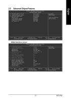
Gigabyte C7V7-CSI Manual - Page 28
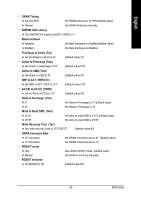
AGP & P2P Bridge Control, CPU & PCI Bus Control, Current, FSB Frequency, DRAM Frequency,
 |
View all Gigabyte C7V7-CSI manuals
Add to My Manuals
Save this manual to your list of manuals |
Page 28 highlights
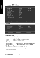
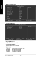
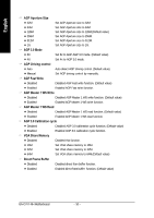
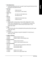
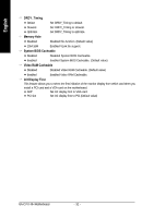
English AGP & P2P Bridge Control Phoenix- AwardBIOS CMOS Setup Utility AGP & P2P Bridge Control AGP Aperture Size AGP3.0 Mode AGP Driving Control x AGP Driving Value AGP Fast Write AGP Master 1 WS Write AGP Master 1 WS Read AGP 3.0 Calibration cycle VGA Share Memory Size Direct Frame Buffer Select Display Device Panel Type Outport Port Dithering TV-Layout TV-type TV-connector [128M] [8X] [Auto] DA [Disabled] [Enabled] [Enabled] [Disabled] [64M] [Enabled] [CRT] [07] [DI0] [Disabled] [Default] [NTSC] [CVBS] Item Help Menu Level : Move Enter: Select F5: Previous Values +/-/PU/PD: Value F10: Save F6: Fail-Safe Defaults ESC: Exit F1: General Help F7: Optimized Defaults CPU & PCI Bus Control PCI Master 0 WS Write PCI Delay Transaction VLink mode selection VLink 8x Support DRDY_Timing Phoenix- AwardBIOS CMOS Setup Utility CPU & PCI Bus Control [Enabled] [Enabled] [By Auto] [Enabled] [Default] Item Help Menu Level : Move Enter: Select F5: Previous Values +/-/PU/PD: Value F10: Save F6: Fail-Safe Defaults Current FSB Frequency Detect front side bus automatically. Current DRAM Frequency Detect DRAM fruquency automatically. DRAM Clock By SPD Set DRAM Clock by SPD.(Default Value) 200MHz 266MHz 333MHz Set DRAM Clock to 200MHz. Set DRAM Clock to 266MHz. Set DRAM Clock to 333MHz. ESC: Exit F1: General Help F7: Optimized Defaults GA-C7V7-RH Motherboard - 28 -
-
 1
1 -
2
-
3
-
4
-
5
-
6
-
7
-
8
-
9
-
10
-
11
-
12
-
13
-
14
-
15
-
16
-
17
-
18
-
19
-
20
-
21
-
22
-
 23
23 -
 24
24 -
 25
25 -
 26
26 -
 27
27 -
 28
28 -
 29
29 -
 30
30 -
 31
31 -
 32
32 -
 33
33 -
34
-
35
-
36
-
37
-
38
-
39
-
40
-
41
-
42
-
43
-
44
-
45
-
46
-
47
-
48
 |
 |