Gigabyte GA-VM900MC Manual - Page 8
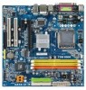
Block Diagram - bios
 |
View all Gigabyte GA-VM900MC manuals
Add to My Manuals
Save this manual to your list of manuals |
Page 8 highlights
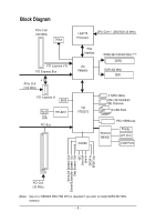
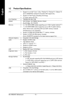
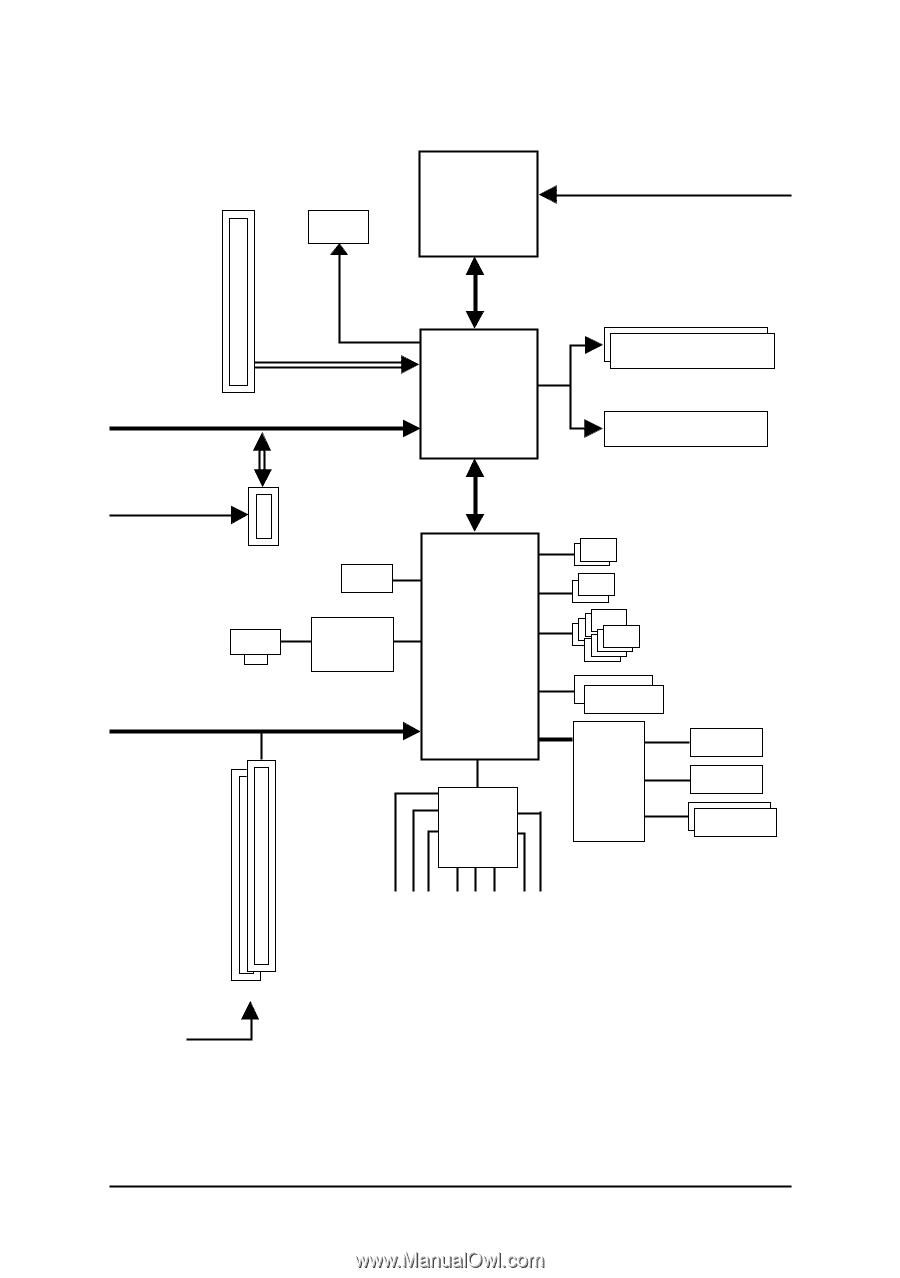
Block Diagram PCIe CLK (100 MHz) D-Sub PCI Express x16 PCI Express Bus x1 PCIe CLK (100 MHz) PCI Express x1 BIOS RJ45 LAN PCI Bus RTL8201 LGA775 Processor CPU CLK+/- (266/200/133 MHz) Host Interface VIA P4M900 DDR2 667/533/400 MHz (Note) DDR2 DDR 400 MHz DDR VIA VT8237S CODEC 2 SATA 3Gb/s ATA-133/100/66/33 IDE Channels 8 USB Ports Winbond W83627 PS/2 KB/Mouse Floppy LPT Port COM Ports Surround Speaker Out Center/Subwoofer Speaker Out Side Speaker Out MIC Line-Out Line-In SPDIF In SPDIF Out 2 PCI PCI CLK (33 MHz) (Note) Use of a 1066/800 MHz FSB CPU is required if you wish to install DDR2 667 MHz memory. - 8 -
-
 1
1 -
2
-
 3
3 -
 4
4 -
 5
5 -
 6
6 -
 7
7 -
 8
8 -
 9
9 -
 10
10 -
 11
11 -
 12
12 -
 13
13 -
14
-
15
-
16
-
17
-
18
-
19
-
20
-
21
-
22
-
23
-
24
-
25
-
26
-
27
-
28
-
29
-
30
-
31
-
32
-
33
-
34
-
35
-
36
-
37
-
38
-
39
-
40
-
41
-
42
-
43
-
44
-
45
-
46
-
47
-
48
-
49
-
50
-
51
-
52
-
53
-
54
-
55
-
56
-
57
-
58
-
59
-
60
-
61
-
62
-
63
-
64
-
65
-
66
-
67
-
68
-
69
-
70
-
71
-
72
-
73
-
74
-
75
-
76
-
77
-
78
-
79
-
80
-
81
-
82
-
83
-
84
-
85
-
86
-
87
-
88
 |
 |
- 8 -
Block Diagram
LGA775
Processor
Host
Interface
VIA
P4M900
DDR2 667/533/400 MHz
(Note)
2 PCI
PCI Bus
PCI Express Bus
DDR2
PCI CLK
(33 MHz)
PCIe CLK
(100 MHz)
PCI Express x16
8 USB Ports
ATA-133/100/66/33
IDE Channels
RTL8201
Floppy
PS/2 KB/Mouse
LPT Port
CPU CLK+/- (266/200/133 MHz)
D-Sub
Center/Subwoofer Speaker Out
Line-Out
MIC
Line-In
SPDIF In
SPDIF Out
Side Speaker Out
Surround Speaker Out
CODEC
(Note)
Use of a 1066/800 MHz FSB CPU is required if you wish to install DDR2 667 MHz
memory.
Winbond
W83627
VIA
VT8237S
COM Ports
2 SATA 3Gb/s
LAN
RJ45
x1
PCI Express x1
PCIe CLK
(100 MHz)
BIOS
DDR 400 MHz
DDR