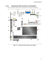
Intel D510MO Product Specification - Page 45
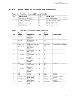
Signal Tables for the Connectors and Headers, Table 13., Serial Port Header COM 1 and COM 2
 |
View all Intel D510MO manuals
Add to My Manuals
Save this manual to your list of manuals |
Page 45 highlights
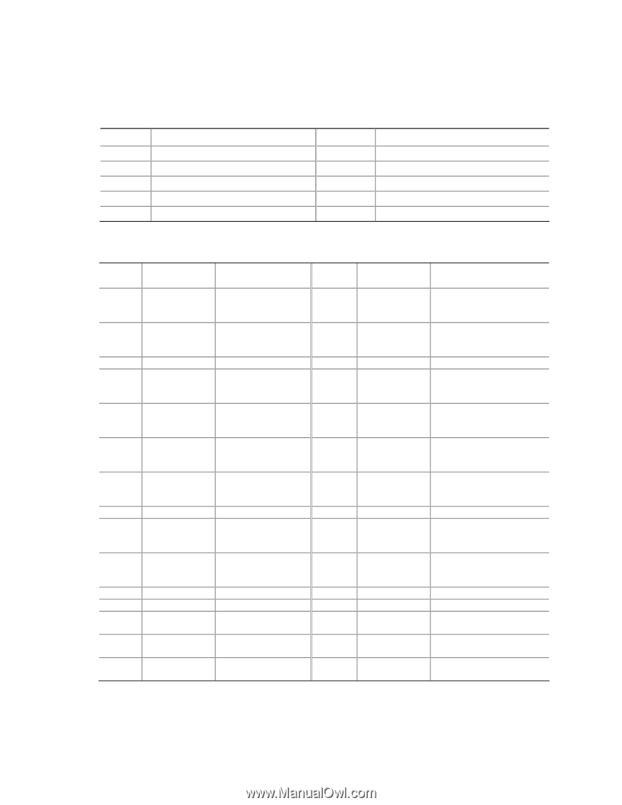
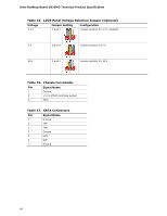
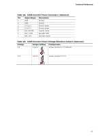
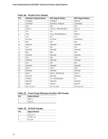
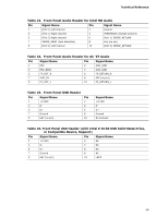
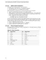
Technical Reference 2.2.2.1 Signal Tables for the Connectors and Headers Table 13. Serial Port Header (COM 1 and COM 2) Pin Signal Name Pin Signal Name 1 DCD (Data Carrier Detect) 3 TXD# (Transmit Data) 5 Ground 7 RTS (Request To Send) 9 RI (Ring Indicator) 2 RXD# (Receive Data) 4 DTR (Data Terminal Ready) 6 DSR (Data Set Ready) 8 CTS (Clear To Send) 10 Key (no pin) Table 14. LVDS Data Connector - 30-Pin (Optional) Pin 1 3 5 7 9 11 13 15 17 19 21 23 25 27 29 Signal Name LA_CLKN LA_CLKP EDID_3.3V LA_DATAN0 LA_DATAP0 LA_DATAN1 LA_DATAP1 GND LA_DATAN2 LA_DATAP2 GND GND 3.3 V/5 V/12 V 3.3 V/5 V/12 V EDID_CLK Description LVDS Channel A diff clock output negative LVDS Channel A diff clock output positive Power for EDID ROM LVDS Channel A diff data output - negative LVDS Channel A diff data output - positive LVDS Channel A diff data output - negative LVDS Channel A diff data output - positive Ground LVDS Channel A diff data output - negative LVDS Channel A diff data output - positive Ground Ground Selectable LCD power output Selectable LCD power output EDID/DDC clock signal Pin 2 4 6 8 10 12 14 16 18 20 22 24 26 28 30 Signal Name NC Description NC EDID_GND NC Ground for EDID signaling NC NC NC GND NC Ground NC GND GND 3.3 V/5 V/12 V 3.3 V/5 V/12 V EDID_DATA Ground Ground Selectable LCD power output Selectable LCD power output EDID/DDC data signal 45
-
 1
1 -
2
-
3
-
4
-
5
-
6
-
7
-
8
-
9
-
10
-
11
-
12
-
13
-
14
-
15
-
16
-
17
-
18
-
19
-
20
-
21
-
22
-
23
-
24
-
25
-
26
-
27
-
28
-
29
-
30
-
31
-
32
-
33
-
34
-
35
-
36
-
37
-
38
-
39
-
 40
40 -
 41
41 -
 42
42 -
 43
43 -
 44
44 -
 45
45 -
 46
46 -
 47
47 -
 48
48 -
 49
49 -
 50
50 -
51
-
52
-
53
-
54
-
55
-
56
-
57
-
58
-
59
-
60
-
61
-
62
-
63
-
64
-
65
-
66
-
67
-
68
-
69
-
70
-
71
-
72
-
73
-
74
-
75
-
76
-
77
-
78
-
79
-
80
-
81
-
82
-
83
-
84
-
85
-
86
-
87
-
88
-
89
-
90
-
91
-
92
 |
 |