Intel E6300 Data Sheet - Page 19
Table 5., Processor V, Static and Transient Tolerance
 |
UPC - 735858184649
View all Intel E6300 manuals
Add to My Manuals
Save this manual to your list of manuals |
Page 19 highlights
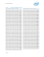
Electrical Specifications Table 5. 1. Each processor is programmed with a maximum valid voltage identification value (VID), which is set at manufacturing and can not be altered. Individual maximum VID values are calibrated during manufacturing such that two processors at the same frequency may have different settings within the VID range. Note that this differs from the VID employed by the processor during a power management event (Thermal Monitor 2, Enhanced Intel SpeedStep technology, or Extended HALT State). 2. Unless otherwise noted, all specifications in this table are based on estimates and simulations or empirical data. These specifications will be updated with characterized data from silicon measurements at a later date. 3. These voltages are targets only. A variable voltage source should exist on systems in the event that a different voltage is required. See Section 2.3 and Table 2 for more information. 4. The voltage specification requirements are measured across VCC_SENSE and VSS_SENSE lands at the socket with a 100 MHz bandwidth oscilloscope, 1.5 pF maximum probe capacitance, and 1 M minimum impedance. The maximum length of ground wire on the probe should be less than 5 mm. Ensure external noise from the system is not coupled into the oscilloscope probe. 5. See Table 5 and Figure 1, for the minimum, typical, and maximum VCC allowed for a given current. The processor should not be subjected to any VCC and ICC combination wherein VCC exceeds VCC_MAX for a given current. 6. ICC_MAX specification is based on VCC_MAX loadline. See Figure 1 for details. 7. VTT must be provided using a separate voltage source and not be connected to VCC. This specification is measured at the land. 8. Baseboard bandwidth is limited to 20 MHz. 9. This is the maximum total current drawn from the VTT plane by only the processor. This specification does not include the current coming from on-board termination (RTT), through the signal line. See the Voltage Regulator Design Guide to determine the total ITT drawn by the system. This parameter is based on design characterization and is not tested. 10. Adherence to the voltage specifications for the processor are required to ensure reliable processor operation. Processor VCC Static and Transient Tolerance ICC (A) Voltage Deviation from VID Setting (V)1, 2, 3, 4 Maximum Voltage 1.65 m Typical Voltage 1.73 m Minimum Voltage 1.80 m 0 0.000 -0.019 -0.038 5 -0.008 -0.028 -0.047 10 -0.017 -0.036 -0.056 15 -0.025 -0.045 -0.065 20 -0.033 -0.054 -0.074 25 -0.041 -0.062 -0.083 30 -0.050 -0.071 -0.092 35 -0.058 -0.079 -0.101 40 -0.066 -0.088 -0.110 45 -0.074 -0.097 -0.119 50 -0.083 -0.105 -0.128 55 -0.091 -0.114 -0.137 60 -0.099 -0.123 -0.146 65 -0.107 -0.131 -0.155 70 -0.116 -0.140 -0.164 75 -0.124 -0.148 -0.173 NOTES: 1. The loadline specification includes both static and transient limits except for overshoot allowed as shown in Section 2.6.3. 2. This table is intended to aid in reading discrete points on Figure 1. Datasheet 19
-
 1
1 -
2
-
3
-
4
-
5
-
6
-
7
-
8
-
9
-
10
-
11
-
12
-
13
-
 14
14 -
 15
15 -
 16
16 -
 17
17 -
 18
18 -
 19
19 -
 20
20 -
 21
21 -
 22
22 -
 23
23 -
 24
24 -
25
-
26
-
27
-
28
-
29
-
30
-
31
-
32
-
33
-
34
-
35
-
36
-
37
-
38
-
39
-
40
-
41
-
42
-
43
-
44
-
45
-
46
-
47
-
48
-
49
-
50
-
51
-
52
-
53
-
54
-
55
-
56
-
57
-
58
-
59
-
60
-
61
-
62
-
63
-
64
-
65
-
66
-
67
-
68
-
69
-
70
-
71
-
72
-
73
-
74
-
75
-
76
-
77
-
78
-
79
-
80
-
81
-
82
-
83
-
84
-
85
-
86
-
87
-
88
-
89
-
90
-
91
-
92
-
93
-
94
-
95
-
96
-
97
-
98
-
99
-
100
 |
 |
