Intel E6300 Data Sheet - Page 54
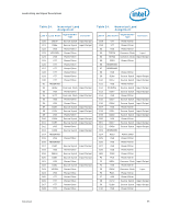
Table 24., Numerical Land, Assignment
 |
UPC - 735858184649
View all Intel E6300 manuals
Add to My Manuals
Save this manual to your list of manuals |
Page 54 highlights
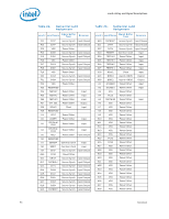
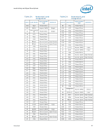
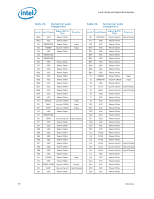
Land Listing and Signal Descriptions Table 24. Numerical Land Assignment Land # Land Name Signal Buffer Type Direction A2 A3 A4 A5 A6 A7 A8 A9 A10 A11 A12 A13 A14 A15 A16 A17 A18 A19 A20 A21 A22 A23 A24 A25 A26 A27 A28 A29 A30 B1 B2 B3 B4 B5 B6 B7 B8 B9 B10 VSS Power/Other RS2# Common Clock Input D02# Source Synch Input/Output D04# Source Synch Input/Output VSS Power/Other D07# Source Synch Input/Output DBI0# Source Synch Input/Output VSS Power/Other D08# Source Synch Input/Output D09# Source Synch Input/Output VSS Power/Other COMP0 Power/Other Input D50# Source Synch Input/Output VSS Power/Other DSTBN3# Source Synch Input/Output D56# Source Synch Input/Output VSS Power/Other D61# Source Synch Input/Output RESERVED VSS Power/Other D62# Source Synch Input/Output VCCA Power/Other FC23 Power/Other VTT Power/Other VTT Power/Other VTT Power/Other VTT Power/Other VTT Power/Other VTT Power/Other VSS Power/Other DBSY# Common Clock Input/Output RS0# Common Clock Input D00# Source Synch Input/Output VSS Power/Other D05# Source Synch Input/Output D06# Source Synch Input/Output VSS Power/Other DSTBP0# Source Synch Input/Output D10# Source Synch Input/Output Table 24. Numerical Land Assignment Land # Land Name Signal Buffer Type Direction B11 B12 B13 B14 B15 B16 B17 B18 B19 B20 B21 B22 B23 B24 B25 B26 B27 B28 B29 B30 C1 C2 C3 C4 C5 C6 C7 C8 C9 C10 C11 C12 C13 C14 C15 C16 C17 C18 C19 VSS D13# COMP8 VSS D53# D55# VSS D57# D60# VSS D59# D63# VSSA VSS VTT VTT VTT VTT VTT VTT DRDY# BNR# LOCK# VSS D01# D03# VSS DSTBN0# FC41 VSS D11# D14# VSS D52# D51# VSS DSTBP3# D54# VSS Power/Other Source Synch Input/Output Power/Other Input Power/Other Source Synch Input/Output Source Synch Input/Output Power/Other Source Synch Input/Output Source Synch Input/Output Power/Other Source Synch Input/Output Source Synch Input/Output Power/Other Power/Other Power/Other Power/Other Power/Other Power/Other Power/Other Power/Other Common Clock Input/Output Common Clock Input/Output Common Clock Input/Output Power/Other Source Synch Input/Output Source Synch Input/Output Power/Other Source Synch Input/Output Power/Other Power/Other Source Synch Input/Output Source Synch Input/Output Power/Other Source Synch Input/Output Source Synch Input/Output Power/Other Source Synch Input/Output Source Synch Input/Output Power/Other 54 Datasheet
-
 1
1 -
2
-
3
-
4
-
5
-
6
-
7
-
8
-
9
-
10
-
11
-
12
-
13
-
14
-
15
-
16
-
17
-
18
-
19
-
20
-
21
-
22
-
23
-
24
-
25
-
26
-
27
-
28
-
29
-
30
-
31
-
32
-
33
-
34
-
35
-
36
-
37
-
38
-
39
-
40
-
41
-
42
-
43
-
44
-
45
-
46
-
47
-
48
-
 49
49 -
 50
50 -
 51
51 -
 52
52 -
 53
53 -
 54
54 -
 55
55 -
 56
56 -
 57
57 -
 58
58 -
 59
59 -
60
-
61
-
62
-
63
-
64
-
65
-
66
-
67
-
68
-
69
-
70
-
71
-
72
-
73
-
74
-
75
-
76
-
77
-
78
-
79
-
80
-
81
-
82
-
83
-
84
-
85
-
86
-
87
-
88
-
89
-
90
-
91
-
92
-
93
-
94
-
95
-
96
-
97
-
98
-
99
-
100
 |
 |
