Intel SL8K2 Specification Update - Page 36
FSW May Not Be Completely Restored after Fault on FRSTOR or
 |
UPC - 683728107215
View all Intel SL8K2 manuals
Add to My Manuals
Save this manual to your list of manuals |
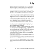
Page 36 highlights
Errata R R11. FSW May Not Be Completely Restored after Page Fault on FRSTOR or FLDENV Instructions Problem: If the FPU operating environment or FPU state (operating environment and register stack) being loaded by an FLDENV or FRSTOR instruction wraps around a 64-KB or 4-GB boundary and a page fault (#PF) or segment limit fault (#GP or #SS) occurs on the instruction near the wrap boundary, the upper byte of the FPU status word (FSW) might not be restored. If the fault handler does not restart program execution at the faulting instruction, stale data may exist in the FSW. Implication: When this erratum occurs, stale data will exist in the FSW. Workaround: Ensure that the FPU operating environment and FPU state do not cross 64-KB or 4-GB boundaries. Alternately, ensure that the page fault handler restarts program execution at the faulting instruction after correcting the paging problem. Status: For the steppings affected, see the Summary Tables of Changes. R12. Processor Issues Inconsistent Transaction Size Attributes for Locked Operation Problem: When the processor is in the Page Address Extension (PAE) mode and detects the need to set the Access and/or Dirty bits in the page directory or page table entries, the processor sends an 8 byte load lock onto the system bus. A subsequent 8 byte store unlock is expected, but instead a 4 byte store unlock occurs. Correct data is provided since only the lower bytes change, however external logic monitoring the data transfer may be expecting an 8-byte store unlock. Implication: No known commercially available chipsets are affected by this erratum. Workaround: None identified. Status: For the steppings affected, see the Summary Tables of Changes. R13. When the Processor Is in the System Management Mode (SMM), Debug Registers May Be Fully Writeable Problem: When in System Management Mode (SMM), the processor executes code and stores data in the SMRAM space. When the processor is in this mode and writes are made to DR6 and DR7, the processor should block writes to the reserved bit locations. Due to this erratum, the processor may not block these writes. This may result in invalid data in the reserved bit locations. Implication: Reserved bit locations within DR6 and DR7 may become invalid. Workaround: Software may perform a read/modify/write when writing to DR6 and DR7 to ensure that the values in the reserved bits are maintained. Status: For the steppings affected, see the Summary Tables of Changes. 36 Intel® Pentium® 4 Processor on 90 nm Process Specification Update
-
 1
1 -
2
-
3
-
4
-
5
-
6
-
7
-
8
-
9
-
10
-
11
-
12
-
13
-
14
-
15
-
16
-
17
-
18
-
19
-
20
-
21
-
22
-
23
-
24
-
25
-
26
-
27
-
28
-
29
-
30
-
 31
31 -
 32
32 -
 33
33 -
 34
34 -
 35
35 -
 36
36 -
 37
37 -
 38
38 -
 39
39 -
 40
40 -
 41
41 -
42
-
43
-
44
-
45
-
46
-
47
-
48
-
49
-
50
-
51
-
52
-
53
-
54
-
55
-
56
-
57
-
58
-
59
-
60
-
61
-
62
-
63
-
64
-
65
-
66
-
67
-
68
-
69
-
70
-
71
-
72
-
73
-
74
-
75
 |
 |