LG MU-42PM12X Service Manual - Page 10
POWER PCB Assy Voltage, Adjustments, DDC Data Input
 |
View all LG MU-42PM12X manuals
Add to My Manuals
Save this manual to your list of manuals |
Page 10 highlights
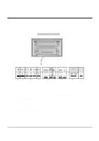
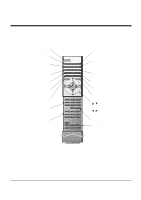
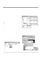
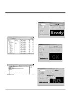
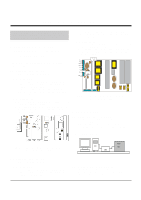
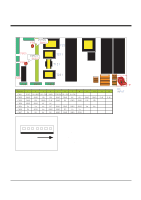
ADJUSTMENT INSTRUCTIONS Each PCB assembly must be checked by Check JIG Set before assembly. (Take special note of the Power PCB, which can easily damage the PDP module) 5. POWER PCB Assy Voltage Adjustments (Va, Vs Voltage Adjustments) 5-1. Test Equipment : D.M.M. 1EA 3) Turn RV501, to adjust the Va voltage to match the value marked on the label on the right/top of the panel. (Deviation; ±0.5V) (2) Vs Adjustment 1) Connect + terminal of D.M.M to Vs pin of P805, connect - terminal to GND pin of P805. 2) Turn RV401, to adjust the Vs voltage to match the value marked on the label on the right/top of the panel. (Deviation; ±0.5V) 5-2. Connection Diagram for Measuring Refer to (Fig 9). 5-3. Adjustment Method for P/No. 3501V00182A/B B/D (1) Va Adjustment 1) After receiving 100% Full White Pattern, HEAT RUN. 2) Connect + terminal of D.M.M to Va pin of P805, connect - terminal to GND pin of P805. 3) Turn RV601, to adjust the Va voltage to match the value marked on the label on the right/top of the panel. (Deviation; ±0.5V) (2) Vs Adjustment 1) Connect + terminal of D.M.M to Vs pin of P805, connect - terminal to GND pin of P805. 2) Turn RV401, to adjust the Vs voltage to match the value marked on the label on the right/top of the panel. (Deviation; ±0.5V) (Fig. 9-2) Connection Diagram of Power Adjustment for Measuring(3501V00187A) 6. DDC Data Input 6-1. Required Test Equipment (1) A jig for adjusting PC, DDC (PC serial to D-sub Connection equipment) (2) S/W for writing DDC (EDID Data Write & Read) (3) D-sub 15P Cable, D-Sub to DVI Connector (Connect to DVI Jack) 6-2. Setting of Device (Fig. 9-1) Connection Diagram of Power Adjustment for Measuring(3501V00182A/B) 5-4. Adjustment Method for P/No. 3501V00187A B/D (1) Va Adjustment 1) After receiving 100% Full White Pattern, HEAT RUN. 2) Connect + terminal of D.M.M to Va pin of P805, connect - terminal to GND pin of P805. (Fig. 10) 6-3. Preparation for Adjustment (1) Set devices as above and turn the PC and jig on. (2) Put S/W for writing DDC (EDID data Write & Read) into operation. (operated in DOS mode.) - 10 -
-
 1
1 -
2
-
3
-
4
-
 5
5 -
 6
6 -
 7
7 -
 8
8 -
 9
9 -
 10
10 -
 11
11 -
 12
12 -
 13
13 -
 14
14 -
 15
15 -
16
-
17
-
18
-
19
-
20
-
21
-
22
-
23
-
24
-
25
-
26
-
27
-
28
-
29
-
30
-
31
-
32
-
33
-
34
-
35
-
36
-
37
-
38
-
39
-
40
-
41
-
42
 |
 |
