MSI P55A User Guide - Page 63
Select whether DRAM timing is controlled by the SPD Serial Presence Detect EE
 |
View all MSI P55A manuals
Add to My Manuals
Save this manual to your list of manuals |
Page 63 highlights
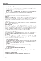
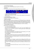
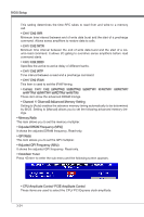
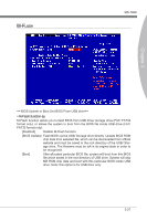
▶ Auto OverClock Technology This item is used to enable/ disable Auto OverClock Technology. ▶ Memory-Z Press to enter the sub-menu and the following screen appears. MS-7668 Chapter 3 ▶ DIMM1~4 Memory SPD Information Press to enter the sub-menu. The sub-menu displays the informations of installed memory. ▶ Current DRAM Channel1~4 Timing It shows the installed DRAM Timing. Read-only. ▶ DRAM Timing Mode Select whether DRAM timing is controlled by the SPD (Serial Presence Detect) EEPROM on the DRAM module. Setting to [Auto] enables DRAM timings and the following "Advance DRAM Configuration" sub-menu to be determined by BIOS based on the configurations on the SPD. Selecting [Manual] allows users to configure the DRAM timings and the following related "Advance DRAM Configuration" sub-menu manually. ▶ Advance DRAM Configuration Press to enter the sub-menu. ▶ CH1/ CH2 1T/2T Memory Timing This item controls the SDRAM command rate. Select [1N] makes SDRAM signal controller to run at 1N (N=clock cycles) rate. Selecting [2N] makes SDRAM signal controller run at 2N rate. ▶ CH1/ CH2 CAS Latency (CL) This controls the CAS latency, which determines the timing delay (in clock cycles) before SDRAM starts a read command after receiving it. ▶ CH1/ CH2 tRCD When DRAM is refreshed, both rows and columns are addressed separately. This setup item allows you to determine the timing of the transition from RAS (row address strobe) to CAS (column address strobe). The less the clock cycles, the faster the DRAM performance. ▶ CH1/ CH2 tRP This setting controls the number of cycles for Row Address Strobe (RAS) to be allowed to precharge. If insufficient time is allowed for the RAS to accumulate its charge before DRAM refresh, refresh may be incomplete and DRAM may fail to retain data. This item applies only when synchronous DRAM is installed in the system. ▶ CH1/ CH2 tRAS This setting determines the time RAS takes to read from and write to memory cell. ▶ CH1/ CH2 tRFC 3-23
-
 1
1 -
2
-
3
-
4
-
5
-
6
-
7
-
8
-
9
-
10
-
11
-
12
-
13
-
14
-
15
-
16
-
17
-
18
-
19
-
20
-
21
-
22
-
23
-
24
-
25
-
26
-
27
-
28
-
29
-
30
-
31
-
32
-
33
-
34
-
35
-
36
-
37
-
38
-
39
-
40
-
41
-
42
-
43
-
44
-
45
-
46
-
47
-
48
-
49
-
50
-
51
-
52
-
53
-
54
-
55
-
56
-
57
-
 58
58 -
 59
59 -
 60
60 -
 61
61 -
 62
62 -
 63
63 -
 64
64 -
 65
65 -
 66
66 -
 67
67 -
 68
68 -
69
-
70
-
71
-
72
-
73
-
74
-
75
-
76
-
77
-
78
-
79
-
80
-
81
-
82
-
83
-
84
-
85
-
86
-
87
-
88
-
89
-
90
-
91
-
92
-
93
-
94
-
95
-
96
-
97
-
98
-
99
-
100
-
101
-
102
 |
 |
