Sharp XL-HP500 Service Manual - Page 43
IC601, VHiLC75341/-1: Audio Processor LC75341
 |
View all Sharp XL-HP500 manuals
Add to My Manuals
Save this manual to your list of manuals |
Page 43 highlights
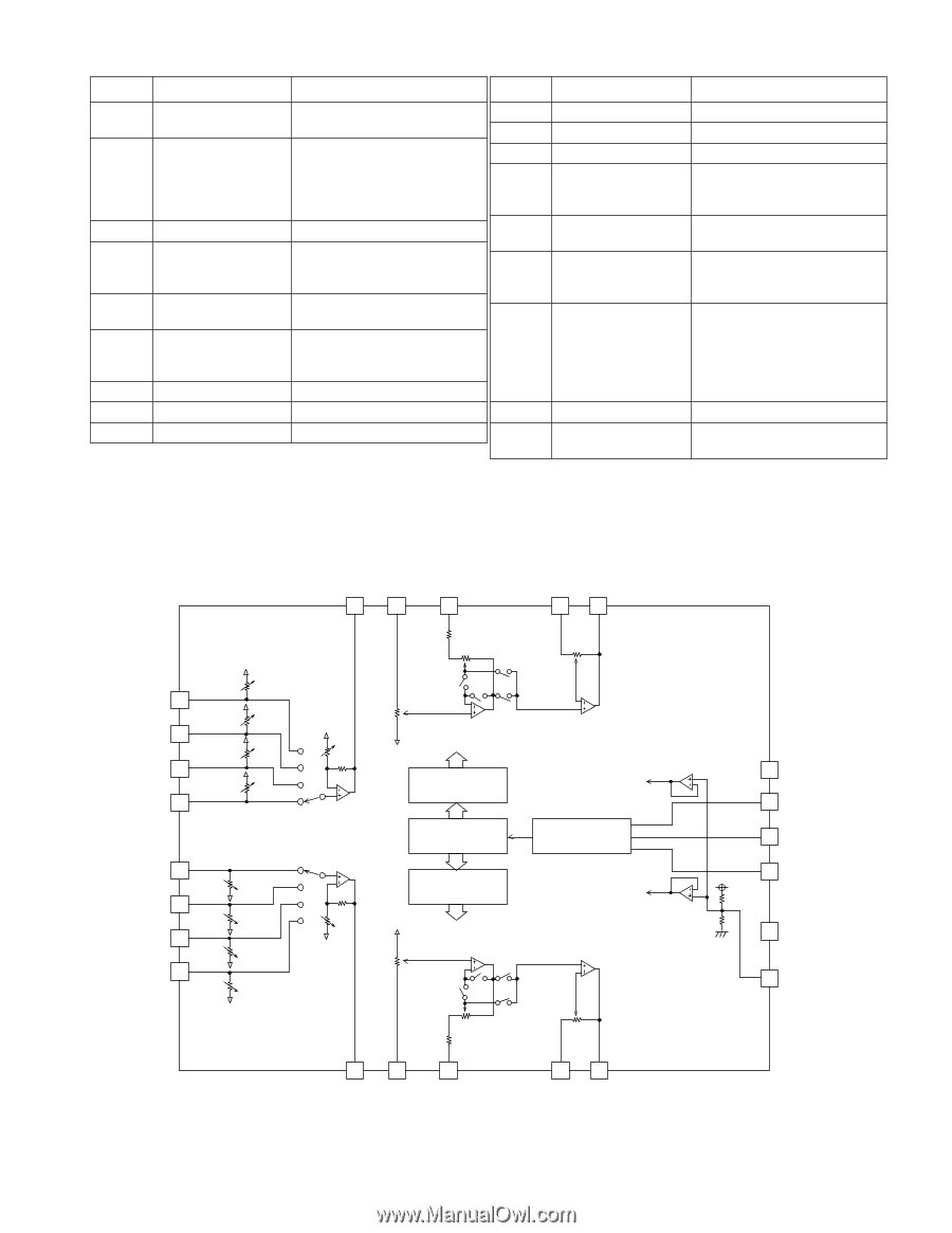
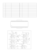
IC601 VHiLC75341/-1: Audio Processor (LC75341) Pin No. Terminal Name 1 DI 2 CE 3 VSS 4 LOUT 5 LBASS 6 LTRE 7 8 9-12 LIN LSEL0 L4-1 Function Pin No. Serial data and clock input pin for control. Chip enable pin. Data written into an internal latch in a timing of "H" to "L". Each analog switch is activated. Data transfer enabled at "H" level. Ground pin. 13-16 17 18 19 20 Bass band filter comprising capacitor and resistor connection 21 pin and bass/treble output pin. Bass band filter comprisingcapacitor and resistor connection pin. 22 Treble band filter comprising capacitor and resistor connection pin. Volume + equaliser output pin Input selector output pin. 23 Input signal pin. 24 Terminal Name R1-4 RSEL0 RIN RTRE RBASS ROUT VREF VDD CLK XL-HP500 Function Input signal pin. Input selector output pin. Volume + equaliser output pin Treble band filter comprising capacitor and resistor connection pin. Bass band filter comprisingcapacitor and resistor connection pin. Bass band filter comprising capacitor and resistor connection pin and bass/treble output pin. 0.5x VDD voltage generation block for analog ground. Capacitor of several 10µF to be connected between VREF and AWSS (VSS) as a countermeasure against power ripple. Supply pin Serial data and clock input pin for control. IC601 VHiLC75341/-1: Audio Processor (LC75341) LSEL0 LIN LTRE LBASS LOUT L4 9 CD L3 10 Tuner L2 11 Tape L1 12 Video R1 13 R2 14 R3 15 R4 16 87 6 54 CONTROL CIRCUIT CONTROL CIRCUIT CONTROL CIRCUIT LVref CCB INTERFACE RVref 17 18 19 20 21 3 VSS 2 CE 1 DI 24 CLK 23 VDD 22 VREF RSEL0 RIN RTRE RBASS ROUT Figure 43 BLOCK DIAGRAM OF IC - 43 -
-
 1
1 -
2
-
3
-
4
-
5
-
6
-
7
-
8
-
9
-
10
-
11
-
12
-
13
-
14
-
15
-
16
-
17
-
18
-
19
-
20
-
21
-
22
-
23
-
24
-
25
-
26
-
27
-
28
-
29
-
30
-
31
-
32
-
33
-
34
-
35
-
36
-
37
-
 38
38 -
 39
39 -
 40
40 -
 41
41 -
 42
42 -
 43
43 -
 44
44 -
 45
45 -
 46
46 -
 47
47 -
 48
48 -
49
-
50
-
51
-
52
-
53
-
54
-
55
-
56
-
57
-
58
-
59
-
60
 |
 |