Sony HCD-NEZ30 Service Manual - Page 19
Circuit Boards Location, Note for Printed Wiring Boards and Schematic Diagrams
 |
View all Sony HCD-NEZ30 manuals
Add to My Manuals
Save this manual to your list of manuals |
Page 19 highlights
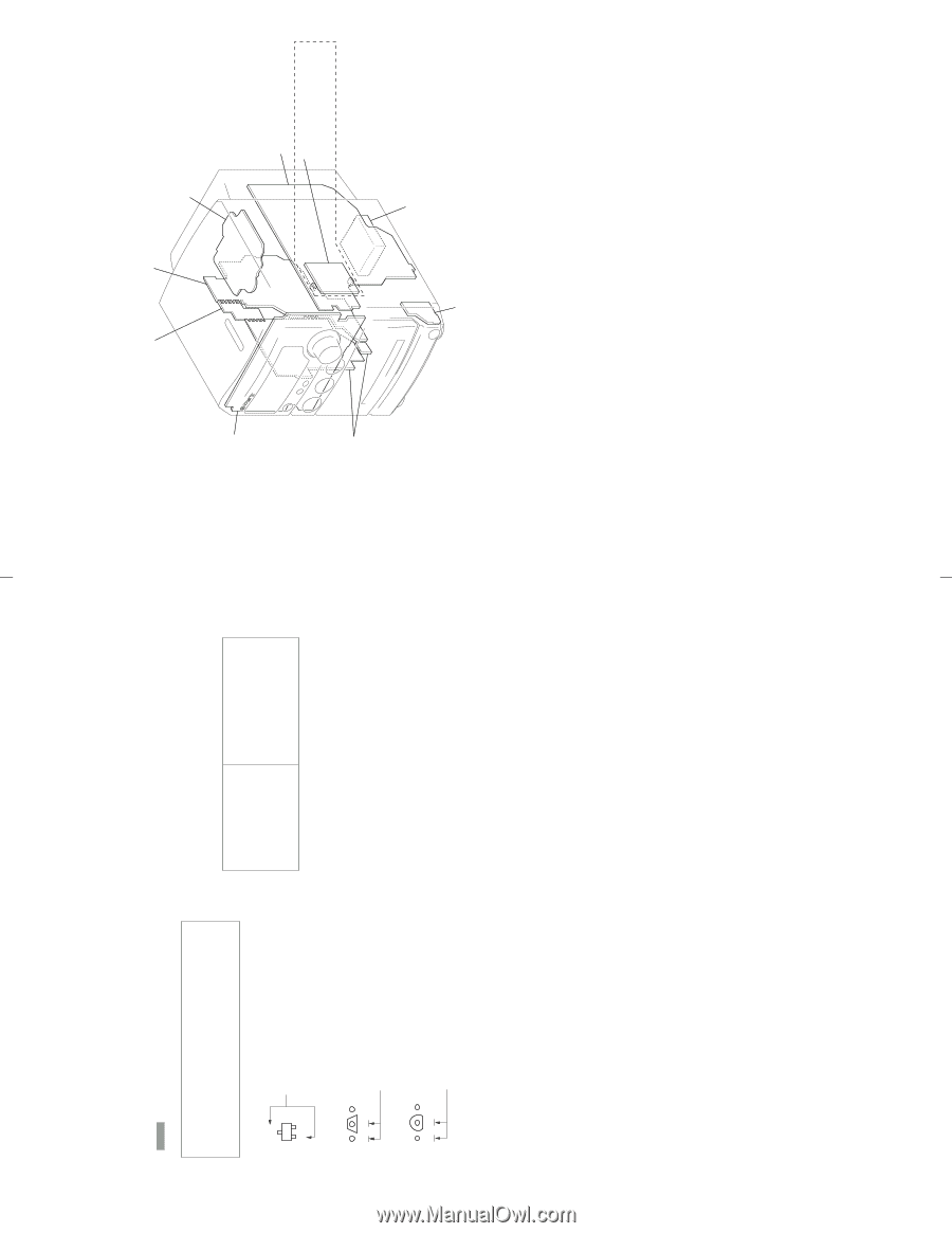
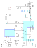
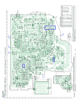
• Note for Printed Wiring Boards and Schematic Diagrams Note on Printed Wiring Board: • X : parts extracted from the component side. • Y : parts extracted from the conductor side. • f : internal component. • : Pattern from the side which enables seeing. (The other layers' patterns are not indicated.) Caution: Pattern face side: (Conductor Side) Parts face side: (Component Side) Parts on the pattern face side seen from the pattern face are indicated. Parts on the parts face side seen from the parts face are indicated. • Indication of transistor C Q These are omitted. BE Q BCE These are omitted. Q BCE These are omitted. Note on Schematic Diagram: • All capacitors are in µF unless otherwise noted. (p: pF) 50 WV or less are not indicated except for electrolytics and tantalums. • All resistors are in Ω and 1/4 W or less unless otherwise specified. • f : internal component. • 2 : nonflammable resistor. • 5 : fusible resistor. • C : panel designation. Note: The components identified by mark 0 or dotted line with mark 0 are critical for safety. Replace only with part number specified. Note: Les composants identifiés par une marque 0 sont critiques pour la sécurité. Ne les remplacer que par une pièce portant le numéro spécifié. • A : B+ Line. • B : B- Line. • Voltages and waveforms are dc with respect to ground under no-signal conditions. - CD Board - no mark : CD PLAY - Other Section - no mark : TUNER ( ) : CD PLAY TAPE PLAY { } : REC • Voltages are taken with a VOM (Input impedance 10 MΩ). Voltage variations may be noted due to normal produc- tion tolerances. • Waveforms are taken with a oscilloscope. Voltage variations may be noted due to normal produc- tion tolerances. • Circled numbers refer to waveforms. • Signal path. F : TUNER J : CD PLAY E : TAPE PLAY j : REC f : AUX IN • Abbreviation AR : Argentina model CND : Canadian model E51 : Chilean and Peruvian models EE : East European model MX : Mexican model • Circuit Boards Location PANEL board DC board HCD-NEZ30 Ver. 1.5 CONNECT board AC board CD board MAIN board SHIELD board (EXCEPT UK, East European) HEAD PHONE board TUNER UNIT HCD-NEZ30 19 19
-
 1
1 -
2
-
3
-
4
-
5
-
6
-
7
-
8
-
9
-
10
-
11
-
12
-
13
-
 14
14 -
 15
15 -
 16
16 -
 17
17 -
 18
18 -
 19
19 -
 20
20 -
 21
21 -
 22
22 -
 23
23 -
 24
24 -
25
-
26
-
27
-
28
-
29
-
30
-
31
-
32
-
33
-
34
-
35
-
36
-
37
-
38
-
39
-
40
-
41
-
42
-
43
-
44
-
45
-
46
-
47
-
48
-
49
-
50
-
51
 |
 |