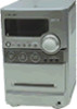
Sony HCD-NEZ30 Service Manual - Page 32
Pin No., Pin Name, Description
 |
View all Sony HCD-NEZ30 manuals
Add to My Manuals
Save this manual to your list of manuals |
Page 32 highlights
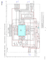
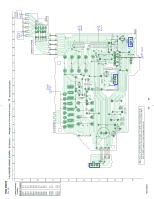
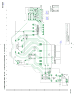
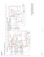
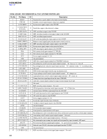
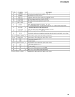
HCD-NEZ30 Pin No. 48 49 50 51 52 53 54 55 56 57 58 59 60 61 62 63 64 65 66 67 68 69 70 71 72 73 74 75 76 77 78 79 80 81 82 83 84 85 86 87 88 89 90 91 92 93 94 95 96 Pin Name AVDD0 AVSS0 E F TEI TEO FEI FEO VC A B C D AVDD4 RFDCO PDSENS AC_SUM EQ_IN LD PD RFC AVSS4 RFACO RFACI AVDD3 BIAS ASYI ASYO VPCO VCTL AVSS3 CLTV FILO FILI PCO SVSS SVDD SSTB-MP3 VDD VSS TEST1 DATA CLK2 SVSS SVDD JTAGTCK JTAGTDI JTAGTDO JTAGTMS I/O Description - Power supply terminal (+3.3V) - Ground terminal I E signal input from the optical pick-up block I F signal input from the optical pick-up block I Tracking error signal input terminal O Tracking error signal output terminal I Focus error signal input terminal O Focus error signal output terminal O Middle point voltage output terminal I A signal input from the optical pick-up block I B signal input from the optical pick-up block I C signal input from the optical pick-up block I D signal input from the optical pick-up block - Power supply terminal (+3.3V) O Not used I Not used O RFAC summing amplifier signal output terminal I RF equalizer circuit input terminal O Laser diode on/off control signal output to the automatic power control circuit "L": laser off, "H": laser on I Light amount monitor input from the optical pick-up block laser diode I Equalizer cut off frequency adjustment terminal - Ground terminal O EFM signal output terminal I EFM signal input terminal - Power supply terminal (+3.3V) I Asymmetry circuit constant current input terminal I Playback EFM asymmetry comparator voltage input terminal O Playback EFM full-swing output terminal O Charge pump output terminal for broad-band EFM PLL I VCO2 control voltage input terminal for broad-band EFM PLL - Ground terminal I VCO1 control voltage input terminal for multiplier O Filter output terminal for master PLL I Filter input terminal for master PLL O Charge pump output terminal for master PLL - Ground terminal - Power supply terminal (+1.8V) I MP3 standby on/off control signal input terminal "L": standby Not used - Power supply terminal (+1.8V) - Ground terminal I Test terminal Normally: fixed at "L" I CD serial data input from the system controller I MP3 serial data transfer clock signal input from the system controller - Ground terminal - Power supply terminal (+2.5V) - Not used - Not used - Not used - Not used 32
-
 1
1 -
2
-
3
-
4
-
5
-
6
-
7
-
8
-
9
-
10
-
11
-
12
-
13
-
14
-
15
-
16
-
17
-
18
-
19
-
20
-
21
-
22
-
23
-
24
-
25
-
26
-
 27
27 -
 28
28 -
 29
29 -
 30
30 -
 31
31 -
 32
32 -
 33
33 -
 34
34 -
 35
35 -
 36
36 -
 37
37 -
38
-
39
-
40
-
41
-
42
-
43
-
44
-
45
-
46
-
47
-
48
-
49
-
50
-
51
 |
 |
