Sony HCD-NEZ30 Service Manual - Page 3

Hcd-nez30, Servicing, Notes - schematic

Page 3 highlights

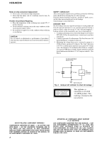
TABLE OF CONTENTS 1. SERVICING NOTES 3 2. GENERAL 6 3. DISASSEMBLY 3-1. Disassembly Flow 8 3-2. Cabinet 8 3-3. Cabinet (Top) Section 9 3-4. Base Unit (BU-K8BD83S-WOD 9 3-5. Front Panel Section 10 3-6. Mechanical Deck (CMAL5Z235A 10 3-7. MAIN Board 11 3-8. Tuner (FM/AM 11 4. TEST MODE 12 5. MECHANICAL ADJUSTMENTS 13 6. ELECTRICAL ADJUSTMENTS 14 7. DIAGRAMS 7-1. Block Diagram - CD SERVO Section 17 7-2. Block Diagram - MAIN Section 18 7-3. Printed Wiring Board - CD Board 20 7-4. Schematic Diagram - CD Board 21 7-5. Printed Wiring Boards - MAIN Section 22 7-6. Schematic Diagram - MAIN Section (1/2 23 7-7. Schematic Diagram - MAIN Section (2/2 24 7-8. Printed Wiring Board - PANEL Board 26 7-9. Schematic Diagram - PANEL Board 27 7-10. Printed Wiring Boards - DC Section 28 7-11. Printed Wiring Board - AC Board 29 7-12. Schematic Diagram - POWER SUPPLY Section - ........ 30 8. EXPLODED VIEWS 8-1. Cabinet Section 36 8-2. Mechanical Deck Section 37 8-3. Panel Board Section 38 8-4. Cabinet (Top) Section 39 8-5. MAIN Board Section 40 8-6. AC Board, DC Board Section 41 9. ELECTRICAL PARTS LIST 42 Refer to SUPPLEMENT-1 for the MAIN board of printed wiring board, schematic diagram and electrical parts list of except US and Canadian models. When repairing the set of US and Canadian models, refer to either of original service manual/SUPPLEMENT-1 according to the set. Refer to SUPPLEMENT-1 for the CD board of printed wiring board, schematic diagram and electrical parts list of UK and East European models. When repairing the set of except UK and East European models, refer to either of original service manual/SUPPLEMENT-1 according to the set. Refer to SUPPLEMENT-2 for the HEAD PHONE board of printed wiring board, schematic diagram and electrical parts list of UK and East European models. When repairing the set of except UK and East European models, refer to either of original service manual/SUPPLEMENT-2 according to the set. Refer to SUPPLEMENT-3 for the PANEL board of printed wiring board, schematic diagram and electrical parts list of UK and East European models. When repairing the set of except UK and East European models, refer to either of original service manual/SUPPLEMENT-3 according to the set. HCD-NEZ30 SECTION 1 Ver. 1.5 SERVICING NOTES NOTES ON HANDLING THE OPTICAL PICK-UP BLOCK OR BASE UNIT The laser diode in the optical pick-up block may suffer electrostatic break-down because of the potential difference generated by the charged electrostatic load, etc. on clothing and the human body. During repair, pay attention to electrostatic break-down and also use the procedure in the printed matter which is included in the repair parts. The flexible board is easily damaged and should be handled with care. NOTES ON LASER DIODE EMISSION CHECK The laser beam on this model is concentrated so as to be focused on the disc reflective surface by the objective lens in the optical pickup block. Therefore, when checking the laser diode emission, observe from more than 30 cm away from the objective lens. UNLEADED SOLDER Boards requiring use of unleaded solder are printed with the leadfree mark (LF) indicating the solder contains no lead. (Caution: Some printed circuit boards may not come printed with the lead free mark due to their particular size) : LEAD FREE MARK Unleaded solder has the following characteristics. • Unleaded solder melts at a temperature about 40 ˚C higher than ordinary solder. Ordinary soldering irons can be used but the iron tip has to be applied to the solder joint for a slightly longer time. Soldering irons using a temperature regulator should be set to about 350 ˚C. Caution: The printed pattern (copper foil) may peel away if the heated tip is applied for too long, so be careful! • Strong viscosity Unleaded solder is more viscou-s (sticky, less prone to flow) than ordinary solder so use caution not to let solder bridges occur such as on IC pins, etc. • Usable with ordinary solder It is best to use only unleaded solder but unleaded solder may also be added to ordinary solder. 3

  • 1
  • 2
  • 3
  • 4
  • 5
  • 6
  • 7
  • 8
  • 9
  • 10
  • 11
  • 12
  • 13
  • 14
  • 15
  • 16
  • 17
  • 18
  • 19
  • 20
  • 21
  • 22
  • 23
  • 24
  • 25
  • 26
  • 27
  • 28
  • 29
  • 30
  • 31
  • 32
  • 33
  • 34
  • 35
  • 36
  • 37
  • 38
  • 39
  • 40
  • 41
  • 42
  • 43
  • 44
  • 45
  • 46
  • 47
  • 48
  • 49
  • 50
  • 51

3
HCD-NEZ30
SECTION
1
SERVICING
NOTES
TABLE
OF
CONTENTS
1.
SERVICING
NOTES
...............................................
3
2.
GENERAL
...................................................................
6
3.
DISASSEMBLY
3-1.
Disassembly Flow
...........................................................
8
3-2.
Cabinet
.............................................................................
8
3-3.
Cabinet (Top) Section
......................................................
9
3-4.
Base Unit (BU-K8BD83S-WOD)
...................................
9
3-5.
Front Panel Section
.........................................................
10
3-6.
Mechanical Deck (CMAL5Z235A)
................................
10
3-7.
MAIN Board
....................................................................
11
3-8.
Tuner (FM/AM)
...............................................................
11
4.
TEST
MODE
..............................................................
12
5.
MECHANICAL
ADJUSTMENTS
.......................
13
6.
ELECTRICAL
ADJUSTMENTS
.........................
14
7.
DIAGRAMS
7-1.
Block Diagram – CD SERVO Section –
.........................
17
7-2.
Block Diagram – MAIN Section –
..................................
18
7-3.
Printed Wiring Board – CD Board –
...............................
20
7-4.
Schematic Diagram – CD Board –
..................................
21
7-5.
Printed Wiring Boards – MAIN Section –
......................
22
7-6.
Schematic Diagram – MAIN Section (1/2) –
..................
23
7-7.
Schematic Diagram – MAIN Section (2/2) –
..................
24
7-8.
Printed Wiring Board – PANEL Board –
........................
26
7-9.
Schematic Diagram – PANEL Board –
...........................
27
7-10.
Printed Wiring Boards – DC Section –
...........................
28
7-11.
Printed Wiring Board – AC Board –
................................
29
7-12.
Schematic Diagram – POWER SUPPLY Section –
........
30
8.
EXPLODED
VIEWS
8-1.
Cabinet Section
................................................................
36
8-2.
Mechanical Deck Section
................................................
37
8-3.
Panel Board Section
........................................................
38
8-4.
Cabinet (Top) Section
......................................................
39
8-5.
MAIN Board Section
.......................................................
40
8-6.
AC Board, DC Board Section
.........................................
41
9.
ELECTRICAL
PARTS
LIST
................................
42
Ver. 1.5
The laser diode in the optical pick-up block may suffer electrostatic
break-down because of the potential difference generated by the
charged electrostatic load, etc. on clothing and the human body.
During repair, pay attention to electrostatic break-down and also
use the procedure in the printed matter which is included in the
repair parts.
The flexible board is easily damaged and should be handled with
care.
NOTES
ON
HANDLING
THE
OPTICAL
PICK-UP
BLOCK
OR
BASE
UNIT
UNLEADED SOLDER
Boards requiring use of unleaded solder are printed with the lead-
free mark (LF) indicating the solder contains no lead.
(Caution: Some printed circuit boards may not come printed with
the lead free mark due to their particular size)
: LEAD FREE MARK
Unleaded solder has the following characteristics.
Unleaded solder melts at a temperature about 40 ˚C higher
than ordinary solder.
Ordinary soldering irons can be used but the iron tip has to be
applied to the solder joint for a slightly longer time.
Soldering irons using a temperature regulator should be set to
about 350 ˚C.
Caution: The printed pattern (copper foil) may peel away if
the heated tip is applied for too long, so be careful!
Strong viscosity
Unleaded solder is more viscou-s (sticky, less prone to flow)
than ordinary solder so use caution not to let solder bridges
occur such as on IC pins, etc.
Usable with ordinary solder
It is best to use only unleaded solder but unleaded solder may
also be added to ordinary solder.
NOTES
ON
LASER
DIODE
EMISSION
CHECK
The laser beam on this model is concentrated so as to be focused on
the disc reflective surface by the objective lens in the optical pick-
up block. Therefore, when checking the laser diode emission,
observe from more than 30 cm away from the objective lens.
Refer to SUPPLEMENT-1 for the CD board of printed wiring board,
schematic diagram and electrical parts list of UK and East European
models.
When repairing the set of except UK and East European models, refer to
either of original service manual/SUPPLEMENT-1 according to the set.
Refer to SUPPLEMENT-2 for the HEAD PHONE board of printed wiring
board, schematic diagram and electrical parts list of UK and East European
models.
When repairing the set of except UK and East European models, refer to
either of original service manual/SUPPLEMENT-2 according to the set.
Refer to SUPPLEMENT-3 for the PANEL board of printed wiring board,
schematic diagram and electrical parts list of UK and East European
models.
When repairing the set of except UK and East European models, refer to
either of original service manual/SUPPLEMENT-3 according to the set.
Refer to SUPPLEMENT-1 for the MAIN board of printed wiring board,
schematic diagram and electrical parts list of except US and Canadian
models.
When repairing the set of US and Canadian models, refer to either of
original service manual/SUPPLEMENT-1 according to the set.