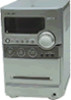
Sony HCD-NEZ30 Service Manual - Page 33
Sony HCD-NEZ30 - Cd Deck Receiver Component Manual
 |
View all Sony HCD-NEZ30 manuals
Add to My Manuals
Save this manual to your list of manuals |
Page 33 highlights
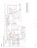
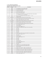
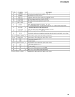
Pin No. 97 98 99 100 101 102 103 104 105 106 107 108 109 110 111 112 113 114 115 116 117 118 119 120 Pin Name TRST VSS VDD IOVDD2 DOUT TEST TES1 IOVSS2 PLLVDD PLLVSS XVSS XTAO XTAI XVDD AVDD1 AOUT1 VREFL AVSS1 AVSS2 VREFR AOUT2 AVDD1 IOVDD0 IOVSS0 I/O Description - Not used - Ground terminal - Power supply terminal (+1.8V) - Power supply terminal (+3.3V) O Digital audio signal output terminal Not used I Test terminal Normally: fixed at "L" I Test terminal Normally: fixed at "L" - Ground terminal - Power supply terminal (+1.8V) - Ground terminal - Ground terminal O System clock output terminal (16.9344 MHz) I System clock input terminal (16.9344 MHz) - Power supply terminal (+1.8V) - Power supply terminal (+3.3V) O L-ch analog audio signal output terminal O L-ch reference voltage output terminal - Ground terminal - Ground terminal O R-ch reference voltage output terminal O R-ch analog audio signal output terminal - Power supply terminal (+3.3V) - Power supply terminal (+3.3V) - Ground terminal HCD-NEZ30 33
-
 1
1 -
2
-
3
-
4
-
5
-
6
-
7
-
8
-
9
-
10
-
11
-
12
-
13
-
14
-
15
-
16
-
17
-
18
-
19
-
20
-
21
-
22
-
23
-
24
-
25
-
26
-
27
-
 28
28 -
 29
29 -
 30
30 -
 31
31 -
 32
32 -
 33
33 -
 34
34 -
 35
35 -
 36
36 -
 37
37 -
 38
38 -
39
-
40
-
41
-
42
-
43
-
44
-
45
-
46
-
47
-
48
-
49
-
50
-
51
 |
 |
