Sony MDS-JE470 Service Manual - Page 37
This Note Is Common For Printed Wiring, Boards And Schematic Diagrams.
 |
View all Sony MDS-JE470 manuals
Add to My Manuals
Save this manual to your list of manuals |
Page 37 highlights
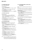
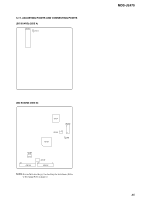
THIS NOTE IS COMMON FOR PRINTED WIRING BOARDS AND SCHEMATIC DIAGRAMS. (In addition to this, the necessary note is printed in each block.) For schematic diagrams. Note: • All capacitors are in µF unless otherwise noted. pF: µµF 50 WV or less are not indicated except for electrolytics and tantalums. • All resistors are in Ω and 1/4 W or less unless otherwise specified. • f : internal component. • C : panel designation. Note: The components identified by mark 0 or dotted line with mark 0 are critical for safety. Replace only with part number specified. Note: Les composants identifiés par une marque 0 sont critiques pour la sécurité. Ne les remplacer que par une piéce portant le numéro spécifié. • A : B+ Line. • B : B- Line. • H : adjustment for repair. • Voltages and waveforms are dc with respect to ground under no-signal (detuned) conditions. no mark : STOP ( ) : PLAY < > : REC ∗ : Impossible to measure • Voltages are taken with a VOM (Input impedance 10 MΩ). Voltage variations may be noted due to normal production tolerances. • Waveforms are taken with a oscilloscope. Voltage variations may be noted due to normal production tolerances. • Circled numbers refer to waveforms. • Signal path. E : PB j : REC p : PB (DIGITAL OUT) l : REC (DIGITAL IN) • Abbreviation CND : Canadian model SP : Singapore model HK : Hong Kong model AUS : Australian model For printed wiring boards. Note: • X : parts extracted from the component side. • Y : parts extracted from the conductor side. • a : Through hole. • b : Pattern from the side which enables seeing. (The other layers' patterns are not indicated.) Caution: Pattern face side: Parts on the pattern face side seen from the (Side B) pattern face are indicated. Parts face side: Parts on the parts face side seen from the (Side A) parts face are indicated. BCE These are omitted. BCE These are omitted. C Q These are omitted. BE • WAVEFORMS - BD Board - 1 IC101 ek (RF) 1.3Vp-p 2 IC101 ef (FE) (Play mode) 0.2Vp-p 3 IC101 wh (TE) (Play mode) 1.6Vp-p 4 IC151 qh (OSCI) 3.1Vp-p 22 nesc 5 IC151 wj (LRCK) 3.2Vp-p 22.6 µsec 6 IC151 wk (XBCK) 3.8Vp-p 354 nsec 7 IC151 o; (FS4) 5.67 µsec 8 IC171 3 3.2Vp-p 1.0Vp-p 22 nsec 37 37 MDS-JE470 - MAIN Board - 1 IC1 qd (XOUT) 100 nsec 2 IC550 qs 2.7Vp-p 22 nsec 2.6Vp-p
-
 1
1 -
2
-
3
-
4
-
5
-
6
-
7
-
8
-
9
-
10
-
11
-
12
-
13
-
14
-
15
-
16
-
17
-
18
-
19
-
20
-
21
-
22
-
23
-
24
-
25
-
26
-
27
-
28
-
29
-
30
-
31
-
 32
32 -
 33
33 -
 34
34 -
 35
35 -
 36
36 -
 37
37 -
 38
38 -
 39
39 -
 40
40 -
 41
41 -
 42
42 -
43
-
44
-
45
-
46
-
47
-
48
-
49
-
50
-
51
-
52
-
53
-
54
-
55
-
56
-
57
-
58
-
59
-
60
-
61
-
62
-
63
-
64
-
65
-
66
-
67
-
68
-
69
-
70
 |
 |
