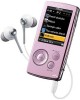
Sony NWZA816P Service Manual - Page 19
Note for Printed Wiring Boards and Schematic Diagrams
 |
UPC - 027242721456
View all Sony NWZA816P manuals
Add to My Manuals
Save this manual to your list of manuals |
Page 19 highlights
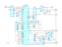
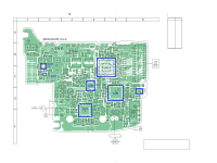
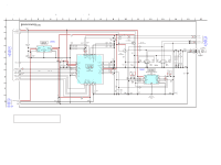
• Note for Printed Wiring Boards and Schematic Diagrams Note on Printed Wiring Board: • Y : parts extracted from the conductor side. • : Pattern from the side which enables seeing. (The other layers' patterns are not indicated.) Caution: Pattern face side: (Side B) Parts face side: (Side A) Parts on the pattern face side seen from the pattern face are indicated. Parts on the parts face side seen from the parts face are indicated. • MAIN board is multi-layer printed board. However, the patterns of intermediate-layers have not been included in diagrams. Note on Schematic Diagram: • All capacitors are in µF unless otherwise noted. (p: pF) 50 WV or less are not indicated except for electrolytics and tantalums. • All resistors are in Ω and 1/4 W or less unless otherwise specified. • C : panel designation. • A : B+ Line. • Power voltage is dc 3.7 V and fed with regulated dc power supply from CN901 pin 1 and pin 2 on the MAIN board. • Voltages are dc with respect to ground under no-signal conditions. no mark : PLAY BACK • Voltages are taken with a VOM (Input impedance 10 MΩ). Voltage variations may be noted due to normal production tolerances. • Signal path. F : AUDIO L : VIDEO • Abbreviation FR : French model NW-A805/A806/A808/NWZ-A815/A816/A818 Ver. 1.2 NW-A805/A806/A808/NWZ-A815/A816/A818 19 19
-
 1
1 -
2
-
3
-
4
-
5
-
6
-
7
-
8
-
9
-
10
-
11
-
12
-
13
-
 14
14 -
 15
15 -
 16
16 -
 17
17 -
 18
18 -
 19
19 -
 20
20 -
 21
21 -
 22
22 -
 23
23 -
 24
24 -
25
-
26
-
27
-
28
-
29
-
30
-
31
-
32
-
33
-
34
-
35
-
36
-
37
-
38
-
39
-
40
-
41
-
42
-
43
-
44
-
45
-
46
-
47
-
48
-
49
-
50
-
51
-
52
 |
 |
