Sony NWZA816P Service Manual - Page 36
W24, W25, SDR_A2, SDR_A1
 |
UPC - 027242721456
View all Sony NWZA816P manuals
Add to My Manuals
Save this manual to your list of manuals |
Page 36 highlights
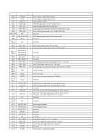
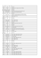
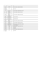
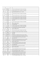
NW-A805/A806/A808/NWZ-A815/A816/A818 Pin No. Pin Name I/O Description U24 C_TCK I Clock signal input terminal for JTAG Not used U25 VPLL O Power supply voltage output terminal U26 CKI I Main system clock input terminal (11.2896MHz) V1 to V3 IO_A - Not used V4, V5, SDR_A6, SDR_A5, V8 SDR_A7 O Address signal output to the 256Mbit SD-RAM V9 GND - Ground terminal V10 CHG_XCHGEN O Charge enable signal output to the charge control V11 NC - Not used V12 to V15 GND - Ground terminal V16 DSP_DET - Not used V17 LCD_BLTCTL O Control signal output to the LCD back light driver V18, V19 NC - Not used V22 C_RTCK I Clock signal input terminal for JTAG Not used V23 C_TRSTZ I Reset signal input terminal for JTAG Not used V24 VPLLIN I Power supply voltage input terminal V25 VDSPIN I Power supply voltage input terminal V26 VDSP - Not used W1 IOGND - Ground terminal W2 LCD_PCI O PCI signal output to the liquid crystal display W3 LCD_PON O PON signal output to the liquid crystal display W4, W5 SDR_A4, SDR_A3 O Address signal output to the 256Mbit SD-RAM W8 CHG_PEN2 O Charge enable signal output to the charge control W9 GND - Ground terminal W10 NC - Not used W11 to W18 GND - Ground terminal W19 WR_ERR - Not used W22 NC - Not used W23 C_TDI I Data input terminal for JTAG Not used W24, W25 IO_B - Not used W26 VLO O Power supply voltage output terminal Y1 IOVDD - Power supply terminal Y2 CHG_ICTL O Charge on/off control signal output to the charge control Y3 HP_XMUTE O Analog muting on/off control signal output terminal Y4, Y5 SDR_A2, SDR_A1 O Address signal output to the 256Mbit SD-RAM Y22, Y23 TM1, TM0 - Not used Y24, Y25 VDD_DSP - Power supply terminal Y26 VHP O Power supply voltage output terminal AA1 CRD_LINEOUT O Selection signal output to the headphone/line selecter AA2 WAKEUP_INT I Wake up signal input terminal AA3 GPIO9 - Not used AA4 SDR_A0 O Address signal output to the 256Mbit SD-RAM AA5 SDR_CLK O Clock signal output to the 256Mbit SD-RAM AA22, AA23 GND - Ground terminal AA24 TM2 - Not used 36
-
 1
1 -
2
-
3
-
4
-
5
-
6
-
7
-
8
-
9
-
10
-
11
-
12
-
13
-
14
-
15
-
16
-
17
-
18
-
19
-
20
-
21
-
22
-
23
-
24
-
25
-
26
-
27
-
28
-
29
-
30
-
 31
31 -
 32
32 -
 33
33 -
 34
34 -
 35
35 -
 36
36 -
 37
37 -
 38
38 -
 39
39 -
 40
40 -
 41
41 -
42
-
43
-
44
-
45
-
46
-
47
-
48
-
49
-
50
-
51
-
52
 |
 |
