Sony NWZA816P Service Manual - Page 32
Pin No., Pin Name, Description
 |
UPC - 027242721456
View all Sony NWZA816P manuals
Add to My Manuals
Save this manual to your list of manuals |
Page 32 highlights
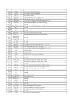
NW-A805/A806/A808/NWZ-A815/A816/A818 Pin No. Pin Name I/O Description C14 NC - Not used C15 SWADP - Not used C16 CAPVBDL - Not used C17 VCCVBAT - Power supply terminal (battery power supply) C18 NC - Not used C19 IO_A - Not used C20 AB0_A5 O Address signal output to the USB controller C21 to C24 NC - Not used C25 AB0_D1 I/O Serial date input/output with the USB controller C26 NC - Not used D1 IDPULLUP - Not used D2 NAND_RBZ0 O Read/busy signal output to the NAND flash memory D3 NAND_ALE O Address latch enable signal output to the NAND flash memory D4 NAND_DA2 I/O Serial date input/output with the NAND flash memory D5 IO_B - Not used D6, D7 VDD_L1 - Power supply terminal D8 GND - Ground terminal D9 NC - Not used D10 GND - Ground terminal D11 to D14 NC - Not used D15 SWVBUS2 - Not used D16 CAPVBSW - Not used D17 VCCVBAT - Power supply terminal (battery power supply) D18 AB0_A3 O Address signal output to the USB controller D19 IO_A - Not used D20 AB0_A6 O Address signal output to the USB controller D21 to D23 NC - Not used D24, D25 AB0_D0, AB0_D2 I/O Serial date input/output with the USB controller D26 NC - Not used E1 DISCHGVBUS - Not used E2 NC - Not used E3 NAND_REZ O Read enable signal output to the NAND flash memory E4 NAND_DA3 I/O Serial date input/output with the NAND flash memory E5 IO_B - Not used E6 NAND_DA5 I/O Serial date input/output with the NAND flash memory E7 NC - Not used E8 NAND_DA7 I/O Serial date input/output with the NAND flash memory E9 NAND_CLE O Command latch enable signal output to the NAND flash memory E10 BATSEL - Not used E11 SWBAT - Not used E12 CAPBTDL - Not used E13 CAPADDL - Not used E14 NC - Not used E15 SWVBUS - Not used E16, E17 NC - Not used E18 AB0_A4 O Address signal output to the USB controller 32
-
 1
1 -
2
-
3
-
4
-
5
-
6
-
7
-
8
-
9
-
10
-
11
-
12
-
13
-
14
-
15
-
16
-
17
-
18
-
19
-
20
-
21
-
22
-
23
-
24
-
25
-
26
-
 27
27 -
 28
28 -
 29
29 -
 30
30 -
 31
31 -
 32
32 -
 33
33 -
 34
34 -
 35
35 -
 36
36 -
 37
37 -
38
-
39
-
40
-
41
-
42
-
43
-
44
-
45
-
46
-
47
-
48
-
49
-
50
-
51
-
52
 |
 |
