ViewSonic VX2262WM Service Manual - Page 22
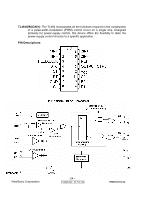
Circuit Diagram, Symbol, Pin Name, Functions
 |
UPC - 766907303919
View all ViewSonic VX2262WM manuals
Add to My Manuals
Save this manual to your list of manuals |
Page 22 highlights
Symbol Pin Name SCK Serial Clock Serial Data SI Input Functions To provide the timing of the serial interface. Commands, addresses, or input data are latched on the rising edge of the clock input, while output data is shifted out on the falling edge of the clock input. To transfer commands, addresses, or data serially into the device. Inputs are latched on the rising edge of the serial clock. SO CE# WP# HOLD# VDD Serial Data Output Chip Enable Write Protect Hold Power Supply To transfer data serially out of the device. Data is shifted out on the falling edge of the serial clock. The device is enabled by a high to low transition on CE#. CE# must remain low for the duration of any command sequence. The Write Protect (WP#) pin is used to enable/disable BPL bit in the status register. To temporarily stop serial communication with SPI flash memory without resetting the device. To provide power supply(3.0-3.6V) VSS Ground Circuit Diagram ViewSonic Corporation - 22 - Confidential - Do Not Cop VX2262wm/wmp
-
 1
1 -
2
-
3
-
4
-
5
-
6
-
7
-
8
-
9
-
10
-
11
-
12
-
13
-
14
-
15
-
16
-
 17
17 -
 18
18 -
 19
19 -
 20
20 -
 21
21 -
 22
22 -
 23
23 -
 24
24 -
 25
25 -
 26
26 -
 27
27 -
28
-
29
-
30
-
31
-
32
-
33
-
34
-
35
-
36
-
37
-
38
-
39
-
40
-
41
-
42
-
43
-
44
-
45
-
46
-
47
-
48
-
49
-
50
-
51
-
52
-
53
-
54
-
55
-
56
-
57
-
58
-
59
-
60
-
61
-
62
-
63
-
64
-
65
-
66
-
67
-
68
-
69
-
70
-
71
-
72
-
73
-
74
-
75
-
76
-
77
-
78
-
79
-
80
-
81
-
82
-
83
 |
 |
