Intel DG965WH Product Specification - Page 7

Regulatory Compliance and Battery Disposal Information, s, Tables - memory support

Page 7 highlights

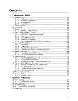
Contents 5 Regulatory Compliance and Battery Disposal Information 5.1 Regulatory Compliance 83 5.1.1 Safety Regulations 83 5.1.2 European Union Declaration of Conformity Statement 84 5.1.3 Product Ecology Statements 86 5.1.4 EMC Regulations 89 5.1.5 Product Certification Markings (Board Level 90 5.2 Battery Disposal Information 91 Figures 1. Major Board Components 12 2. Block Diagram 14 3. Memory Channel and DIMM Configuration 18 4. Dual Channel (Interleaved) Mode Configuration with Two DIMMs 19 5. Dual Channel (Interleaved) Mode Configuration with Three DIMMs ......... 19 6. Dual Channel (Interleaved) Mode Configuration with Four DIMMs 20 7. Single Channel (Asymmetric) Mode Configuration with One DIMM .......... 21 8. Single Channel (Asymmetric) Mode Configuration with Three DIMMs....... 21 9. Flex Mode Configuration with Two DIMMs 22 10. Front/Back Panel Audio Connector Options 30 11. LAN Connector LED Locations 32 12. Thermal Sensors and Fan Headers 34 13. Location of the Standby Power Indicator LED 41 14. Detailed System Memory Address Map 44 15. Back Panel Connectors 51 16. Component-side Connectors and Headers 52 17. Connection Diagram for Front Panel Header 57 18. Connection Diagram for Front Panel USB Headers 59 19. Connection Diagram for IEEE 1394a Header 59 20. Location of the Jumper Block 60 21. Board Dimensions 61 22. I/O Shield Dimensions for Boards with PS/2 Ports 62 23. I/O Shield Dimensions for Boards without PS/2 Ports 63 24. Localized High Temperature Zones 67 Tables 1. Feature Summary 10 2. Manufacturing Options 11 3. Board Components Shown in Figure 1 13 4. Supported Memory Configurations 16 5. Memory Operating Frequencies 17 6. Audio Jack Retasking Support 29 7. LAN Connector LED States 32 8. Effects of Pressing the Power Switch 35 9. Power States and Targeted System Power 36 vii

  • 1
  • 2
  • 3
  • 4
  • 5
  • 6
  • 7
  • 8
  • 9
  • 10
  • 11
  • 12
  • 13
  • 14
  • 15
  • 16
  • 17
  • 18
  • 19
  • 20
  • 21
  • 22
  • 23
  • 24
  • 25
  • 26
  • 27
  • 28
  • 29
  • 30
  • 31
  • 32
  • 33
  • 34
  • 35
  • 36
  • 37
  • 38
  • 39
  • 40
  • 41
  • 42
  • 43
  • 44
  • 45
  • 46
  • 47
  • 48
  • 49
  • 50
  • 51
  • 52
  • 53
  • 54
  • 55
  • 56
  • 57
  • 58
  • 59
  • 60
  • 61
  • 62
  • 63
  • 64
  • 65
  • 66
  • 67
  • 68
  • 69
  • 70
  • 71
  • 72
  • 73
  • 74
  • 75
  • 76
  • 77
  • 78
  • 79
  • 80
  • 81
  • 82
  • 83
  • 84
  • 85
  • 86
  • 87
  • 88
  • 89
  • 90
  • 91
  • 92
  • 93
  • 94

Contents
vii
5
Regulatory Compliance and Battery Disposal Information
5.1
Regulatory Compliance
.....................................................................
83
5.1.1
Safety Regulations
................................................................
83
5.1.2
European Union Declaration of Conformity Statement
................
84
5.1.3
Product Ecology Statements
...................................................
86
5.1.4
EMC Regulations
..................................................................
89
5.1.5
Product Certification Markings (Board Level)
.............................
90
5.2
Battery Disposal Information
.............................................................
91
Figures
1.
Major Board Components
..................................................................
12
2.
Block Diagram
................................................................................
14
3.
Memory Channel and DIMM Configuration
...........................................
18
4.
Dual Channel (Interleaved) Mode Configuration with Two DIMMs
............
19
5.
Dual Channel (Interleaved) Mode Configuration with Three DIMMs
.........
19
6.
Dual Channel (Interleaved) Mode Configuration with Four DIMMs
...........
20
7.
Single Channel (Asymmetric) Mode Configuration with One DIMM
..........
21
8.
Single Channel (Asymmetric) Mode Configuration with Three DIMMs
.......
21
9.
Flex Mode Configuration with Two DIMMs
............................................
22
10. Front/Back Panel Audio Connector Options
..........................................
30
11. LAN Connector LED Locations
............................................................
32
12. Thermal Sensors and Fan Headers
.....................................................
34
13. Location of the Standby Power Indicator LED
.......................................
41
14. Detailed System Memory Address Map
...............................................
44
15. Back Panel Connectors
.....................................................................
51
16. Component-side Connectors and Headers
...........................................
52
17. Connection Diagram for Front Panel Header
........................................
57
18. Connection Diagram for Front Panel USB Headers
................................
59
19. Connection Diagram for IEEE 1394a Header
........................................
59
20. Location of the Jumper Block
.............................................................
60
21. Board Dimensions
...........................................................................
61
22. I/O Shield Dimensions for Boards with PS/2 Ports
................................
62
23. I/O Shield Dimensions for Boards without PS/2 Ports
............................
63
24. Localized High Temperature Zones
.....................................................
67
Tables
1.
Feature Summary
............................................................................
10
2.
Manufacturing Options
.....................................................................
11
3.
Board Components Shown in Figure 1
................................................
13
4.
Supported Memory Configurations
.....................................................
16
5.
Memory Operating Frequencies
.........................................................
17
6.
Audio Jack Retasking Support
...........................................................
29
7.
LAN Connector LED States
................................................................
32
8.
Effects of Pressing the Power Switch
..................................................
35
9.
Power States and Targeted System Power
...........................................
36