LG KU250 Service Manual - Page 21
GSM Transmitter
 |
View all LG KU250 manuals
Add to My Manuals
Save this manual to your list of manuals |
Page 21 highlights
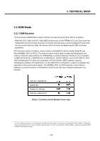
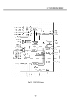
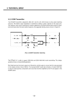
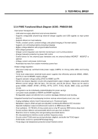
3. TECHNICAL BRIEF 3.2.2 GSM Transmitter The RTR6275 transmitter outputs(DA_HB2_OUT and DA_LB1_OUT)include on-chip output matching inductors. The 50ohm output impedance is achieved by adding a series capacitor at the output pins. The capacitor value may be optimized for specific applications and PCB characteristics based on passband symmetry about the band center frequency, the suggested starting value is shown in Figure1.3. 6pF 51Ω 91Ω 12pF 91Ω 39 Ω 100Ω 100 Ω [Fig 1.3] GSM Transmitter matching The RTR6275 IC is able to support GSM 900 and GSM 1800/1900 mode transmitting. This design guideline shows a tri-band GSM application. Both high-band and low band outputs are followed by resistive pads to ensure that the load presented to the outputs remains close to 50ohm. The low-band GSM Tx path also includes a Tx-band SAW filter to remove noise-spurious components and noise that would be amplified by the PA and appear in the GSM Rx band - 22 -
-
 1
1 -
2
-
3
-
4
-
5
-
6
-
7
-
8
-
9
-
10
-
11
-
12
-
13
-
14
-
15
-
 16
16 -
 17
17 -
 18
18 -
 19
19 -
 20
20 -
 21
21 -
 22
22 -
 23
23 -
 24
24 -
 25
25 -
 26
26 -
27
-
28
-
29
-
30
-
31
-
32
-
33
-
34
-
35
-
36
-
37
-
38
-
39
-
40
-
41
-
42
-
43
-
44
-
45
-
46
-
47
-
48
-
49
-
50
-
51
-
52
-
53
-
54
-
55
-
56
-
57
-
58
-
59
-
60
-
61
-
62
-
63
-
64
-
65
-
66
-
67
-
68
-
69
-
70
-
71
-
72
-
73
-
74
-
75
-
76
-
77
-
78
-
79
-
80
-
81
-
82
-
83
-
84
-
85
-
86
-
87
-
88
-
89
-
90
-
91
-
92
-
93
-
94
-
95
-
96
-
97
-
98
-
99
-
100
-
101
-
102
-
103
-
104
-
105
-
106
-
107
-
108
-
109
-
110
-
111
-
112
-
113
-
114
-
115
-
116
-
117
-
118
-
119
-
120
-
121
-
122
-
123
-
124
-
125
-
126
-
127
-
128
-
129
-
130
-
131
-
132
-
133
-
134
-
135
-
136
-
137
-
138
-
139
-
140
-
141
-
142
-
143
-
144
-
145
-
146
-
147
-
148
-
149
-
150
-
151
-
152
-
153
-
154
-
155
-
156
-
157
-
158
-
159
-
160
-
161
-
162
-
163
-
164
-
165
-
166
-
167
-
168
-
169
-
170
-
171
-
172
-
173
-
174
-
175
 |
 |
