LG KU250 Service Manual - Page 22
UMTS Mode - drivers
 |
View all LG KU250 manuals
Add to My Manuals
Save this manual to your list of manuals |
Page 22 highlights
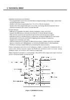
3. TECHNICAL BRIEF 3.3 UMTS Mode 3.3.1 Receiver The UMTS duplexer receiver output is routed to LNA circuits within the RTR6275 device. The UMTS Rx input is provided with an on-chip LNA that amplifies the signal before a second stage filter that provides differential downconverter. This second stage input is configured differentially to optimize second-order intermodulation and common mode rejection performance. The gain of the UMTS frontend amplifier and the UMTS second stage differential amplifier are adjustable, under MSM control, to extend the dynamic range of the receivers. The second stage UMTS Rx amplifiers drive the RF ports of the quadrature RFtobaseband downconverters. The downconverted UMTS Rx baseband outputs are routed to lowpass filters having passband and stopband characteristics suitable for UMTS Rx processing. These filter circuits allow DC offset corrections, and their differential outputs are buffered to interface shared with GSM Rx to the MSM IC. The UMTS baseband outputs are turned off when the RTR6275 is downconverting GSM signals and on when the UMTS is operating. 3.3.2 Transmitter The UMTS Tx path begins with differential baseband signals (I and Q) from the MSM device. These analog input signals are amplified, filtered, and applied to the quadrature up-converter mixers. The upconverter output is amplified by multiple variable gain stages that provide transmit AGC control. The AGC output is filtered and applied to the driver amplifier; this output stage includes an integrated matching inductor that simplifies the external matching network to a single series capacitor to achieve the desired 50-Ω interface. The RTR6275 UMTS output is routed to its power amplifier through a bandpass filter, and delivers fairly high-level signals that are filtered and applied to the PA. Transmit power is delivered from the duplexer to the antenna through the switch module. The transceiver LO synthesizer is contained within the RTR6275 IC with the exception of the off-chip loop filter components and the VC-TCXO. This provides a simplified design for multimode applications. The PLL circuits include a reference divider, phase detector, charge pump, feedback divider, and digital logic generator. UMTS Tx using PLL1, the LO generation and distribution circuits create the necessary LO signals for different frequency converters. The UMTS transmitter also employs the ZIF architecture to translate the signal directly from baseband to RF. This requires FLO to equal FRF, and the RTR6275 IC design achieves this without allowing FVCO to equal FRF. The RTR6275 IC is able to support UMTS 2100/1900 and UMTS 850 mode transmitting. This design guideline shows only UMTS 2100 applications. - 23 -
-
 1
1 -
2
-
3
-
4
-
5
-
6
-
7
-
8
-
9
-
10
-
11
-
12
-
13
-
14
-
15
-
16
-
 17
17 -
 18
18 -
 19
19 -
 20
20 -
 21
21 -
 22
22 -
 23
23 -
 24
24 -
 25
25 -
 26
26 -
 27
27 -
28
-
29
-
30
-
31
-
32
-
33
-
34
-
35
-
36
-
37
-
38
-
39
-
40
-
41
-
42
-
43
-
44
-
45
-
46
-
47
-
48
-
49
-
50
-
51
-
52
-
53
-
54
-
55
-
56
-
57
-
58
-
59
-
60
-
61
-
62
-
63
-
64
-
65
-
66
-
67
-
68
-
69
-
70
-
71
-
72
-
73
-
74
-
75
-
76
-
77
-
78
-
79
-
80
-
81
-
82
-
83
-
84
-
85
-
86
-
87
-
88
-
89
-
90
-
91
-
92
-
93
-
94
-
95
-
96
-
97
-
98
-
99
-
100
-
101
-
102
-
103
-
104
-
105
-
106
-
107
-
108
-
109
-
110
-
111
-
112
-
113
-
114
-
115
-
116
-
117
-
118
-
119
-
120
-
121
-
122
-
123
-
124
-
125
-
126
-
127
-
128
-
129
-
130
-
131
-
132
-
133
-
134
-
135
-
136
-
137
-
138
-
139
-
140
-
141
-
142
-
143
-
144
-
145
-
146
-
147
-
148
-
149
-
150
-
151
-
152
-
153
-
154
-
155
-
156
-
157
-
158
-
159
-
160
-
161
-
162
-
163
-
164
-
165
-
166
-
167
-
168
-
169
-
170
-
171
-
172
-
173
-
174
-
175
 |
 |
