LG KU250 Service Manual - Page 26
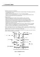
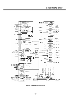
PMIC Functional Block Diagram U300 : PM6650-2M - usb driver
 |
View all LG KU250 manuals
Add to My Manuals
Save this manual to your list of manuals |
Page 26 highlights
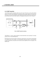
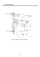
3. TECHNICAL BRIEF 3.5.4 PMIC Functional Block Diagram (U300 : PM6650-2M) • Input power management - Valid external supply attachment and removal detection - Supports unregulated (closed-loop) external charger supplies and USB supplies as input power sources - Supports lithium-ion main batteries - Trickle, constant current, constant voltage, and pulsed charging of the main battery - Supports coin cell backup battery (including charging) - Battery voltage detectors with programmable thresholds - VDD collapse protection - Charger current regulation and real-time monitoring for over-current protection - Charger transistor protection by power limit control - Control drivers for two external pass transistors and one external battery MOSFET - MOSFET is optional - Voltage, current, and power control loops - Automated recovery from sudden momentary power loss • Output voltage regulation - One boost (step-up) switched-mode power supply (SMPS) for driving white LEDs and hosting USBOTG - Three buck (step-down) switched-mode power supplies that efficiently generate MSMC, MSME, and PA (or second MSMC) supply voltages - Supports dynamic voltage scaling (DVS) for MSMC and PA - Eleven low dropout regulator circuits with programmable output voltages, implemented using three different current ratings: 300 mA (two), 150 mA (six), and 50 mA (three). These can be used to power MSMA, MSMP, RFRX1, RFRX2, RFTX, SYNT, TCXO, WLAN, MMC, USB, and RUIM circuits. - All regulators can be individually enabled/disabled for power savings - Low power mode available on MSMA and MSMP regulators - All regulated outputs are derived from a common bandgap reference-close tracking • Integrated handset-level housekeeping functions reduces external parts count, size, cost - Analog multiplexer selects from 8 internal and up to 18 external inputs - Multiplexer output's offset and gain are adjusted, increasing the effective ADC resolution - Adjusted multiplexer output is buffered and routed to an MSM device ADC - Dual oscillators - 32.768 kHz off-chip crystal and on-chip RC assures MSM device sleep clock - Crystal oscillator detector and automated switch-over upon lost oscillation - Real time clock for tracking time and generating associated alarms - On-chip adjustments minimize crystal oscillator frequency errors - Circuits control TCXO warm-up and synchronize, deglitch, and buffer the TCXO signal - TCXO buffer control for optimal QPH/catnap timing - Three-stage over-temperature protection (smart thermal control) - 27 -
-
 1
1 -
2
-
3
-
4
-
5
-
6
-
7
-
8
-
9
-
10
-
11
-
12
-
13
-
14
-
15
-
16
-
17
-
18
-
19
-
20
-
 21
21 -
 22
22 -
 23
23 -
 24
24 -
 25
25 -
 26
26 -
 27
27 -
 28
28 -
 29
29 -
 30
30 -
 31
31 -
32
-
33
-
34
-
35
-
36
-
37
-
38
-
39
-
40
-
41
-
42
-
43
-
44
-
45
-
46
-
47
-
48
-
49
-
50
-
51
-
52
-
53
-
54
-
55
-
56
-
57
-
58
-
59
-
60
-
61
-
62
-
63
-
64
-
65
-
66
-
67
-
68
-
69
-
70
-
71
-
72
-
73
-
74
-
75
-
76
-
77
-
78
-
79
-
80
-
81
-
82
-
83
-
84
-
85
-
86
-
87
-
88
-
89
-
90
-
91
-
92
-
93
-
94
-
95
-
96
-
97
-
98
-
99
-
100
-
101
-
102
-
103
-
104
-
105
-
106
-
107
-
108
-
109
-
110
-
111
-
112
-
113
-
114
-
115
-
116
-
117
-
118
-
119
-
120
-
121
-
122
-
123
-
124
-
125
-
126
-
127
-
128
-
129
-
130
-
131
-
132
-
133
-
134
-
135
-
136
-
137
-
138
-
139
-
140
-
141
-
142
-
143
-
144
-
145
-
146
-
147
-
148
-
149
-
150
-
151
-
152
-
153
-
154
-
155
-
156
-
157
-
158
-
159
-
160
-
161
-
162
-
163
-
164
-
165
-
166
-
167
-
168
-
169
-
170
-
171
-
172
-
173
-
174
-
175
 |
 |
