Sony STR-DB830 Service Manual - Page 21
Schematic Diagram, Power
 |
View all Sony STR-DB830 manuals
Add to My Manuals
Save this manual to your list of manuals |
Page 21 highlights
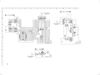
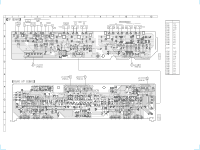
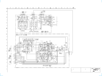
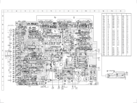
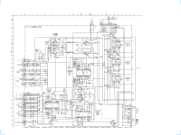
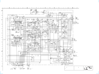
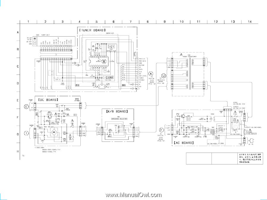
4-16. SCHEMATIC DIAGRAM POWER SECTION • See page 12 for Waveforms. • See page 61 for IC Block Diagrams. STR-DB830/DB930/V929X ANT LEVEL AEP MODEL JR1 TO DIGITAL BOARD (2/3) (PAGE 16) TO MAIN BOARD (2/2) (PAGE 48) - 37 - The components identified by mark ! or dotted line with mark ! are critical for safety. Replace only with part number specified. Les composants identifiés par une marque ! sont critiques pour la sécurité. Ne les remplacer que par une pièce portant le numéro spécifié. - 38 -
-
 1
1 -
2
-
3
-
4
-
5
-
6
-
7
-
8
-
9
-
10
-
11
-
12
-
13
-
14
-
15
-
 16
16 -
 17
17 -
 18
18 -
 19
19 -
 20
20 -
 21
21 -
 22
22 -
 23
23 -
 24
24 -
 25
25 -
 26
26 -
27
-
28
-
29
-
30
-
31
-
32
-
33
-
34
-
35
-
36
-
37
-
38
-
39
-
40
-
41
-
42
-
43
-
44
-
45
-
46
-
47
-
48
-
49
-
50
-
51
-
52
-
53
-
54
-
55
-
56
-
57
-
58
-
59
-
60
-
61
-
62
-
63
-
64
 |
 |
STR-DB830/DB930/V929X
— 37 —
— 38 —
4-16.
SCHEMATIC DIAGRAM
POWER SECTION
• See page 12 for Waveforms.
• See page 61 for IC Block Diagrams.
TO
DIGITAL
BOARD
(2/3)
(PAGE 16)
TO
MAIN
BOARD
(2/2)
(PAGE 48)
JR1
AEP
MODEL
ANT LEVEL
The components identified by
mark
!
or dotted line with mark
!
are critical for safety.
Replace only with part number
specified.
Les composants identifiés par
une marque
!
sont critiques
pour la sécurité.
Ne les remplacer que par une
pièce portant le numéro spécifié.