Sony STR-DB830 Service Manual - Page 32
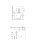
Ic1503, Ak4526a A/d,d/a Converter Digital Board
 |
View all Sony STR-DB830 manuals
Add to My Manuals
Save this manual to your list of manuals |
Page 32 highlights
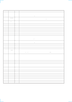
IC1503 AK4526A A/D,D/A CONVERTER (DIGITAL BOARD) Pin No. Pin Name I/O 1 SDOS I I 2 MCLK 3 S/M I 4 BCLK I/O 5 LRCK I/O 6 SDT11 I 7 SDT12 I 8 SDT13 I 9 SDTO O 10 DAUX I 11 DFS I 12 - 13 DEM1 - DEM0 I 14 MCKO O 15 D. 5V - 16 D. GND - 17 PD I 18 TEST I 19 ICKS1 I 20 ICKS0 I 21 CAD1 I 22 CAD0 I 23 LOUT3 O 24 ROUT3 O 25 LOUT2 O 26 ROUT2 O 27 LOUT1 O 28 ROUT1 O 29 LIN- I 30 LIN+ I Description SDTO source select pin "L": internal ADC output, "H": DAUX input ORed with serial control register if P/S = "L" (Connected to ground) MCKO clock frequency select pin "L": MCLK, "H": MCLK/2. ORed with serial control register if P/S = "L" (Connected to ground) Audio data master/slave mode select pin "L": slave mode, "H": master mode (Connected to ground) Audio serial data clock pin Input/output channel clock pin DAC1 audio serial data input pin DAC2 audio serial data input pin DAC3 audio serial data input pin Audio serial data output pin AUX audio serial data input pin (Connected to ground) Double speed sampling mode pin "L": normal speed, "H": double speed ORed with serial control register if P/S = "L" (Connected to ground) De-emphasis pin ORed with serial control register if P/S = "L" (Connected to ground) Master clock output pin (Not used) Digital power supply pin Digital ground pin Power-down & reset pin When "L", the AK4526 is powered-down and the control registers are reset to default state. If the state of P/S, M/S, CAD0-1 changes, then the AK4526 must be reset by PD. X'tal oscillator select/test mode pin "H": X'tal oscillator selected "L": External clock source selected "NC": If pin is floating then test mode is enabled. (Connected to ground) Input clock select 1 pin (Connected to ground) Input clock select 0 pin (Connected to ground) Chip address pin Used during the serial control mode. (Connected to ground) Chip address pin Used during the serial control mode. (Connected to ground) Lch #3 analog output pin Rch #3 analog output pin Lch #2 analog output pin Rch #2 analog output pin Lch #1 analog output pin Rch #1 analog output pin Lch analog negative input pin Lch analog positive input pin - 54 -
-
 1
1 -
2
-
3
-
4
-
5
-
6
-
7
-
8
-
9
-
10
-
11
-
12
-
13
-
14
-
15
-
16
-
17
-
18
-
19
-
20
-
21
-
22
-
23
-
24
-
25
-
26
-
 27
27 -
 28
28 -
 29
29 -
 30
30 -
 31
31 -
 32
32 -
 33
33 -
 34
34 -
 35
35 -
 36
36 -
 37
37 -
38
-
39
-
40
-
41
-
42
-
43
-
44
-
45
-
46
-
47
-
48
-
49
-
50
-
51
-
52
-
53
-
54
-
55
-
56
-
57
-
58
-
59
-
60
-
61
-
62
-
63
-
64
 |
 |
