Sony STR-DB830 Service Manual - Page 28
Pin No., Description, Pin Name
 |
View all Sony STR-DB830 manuals
Add to My Manuals
Save this manual to your list of manuals |
Page 28 highlights
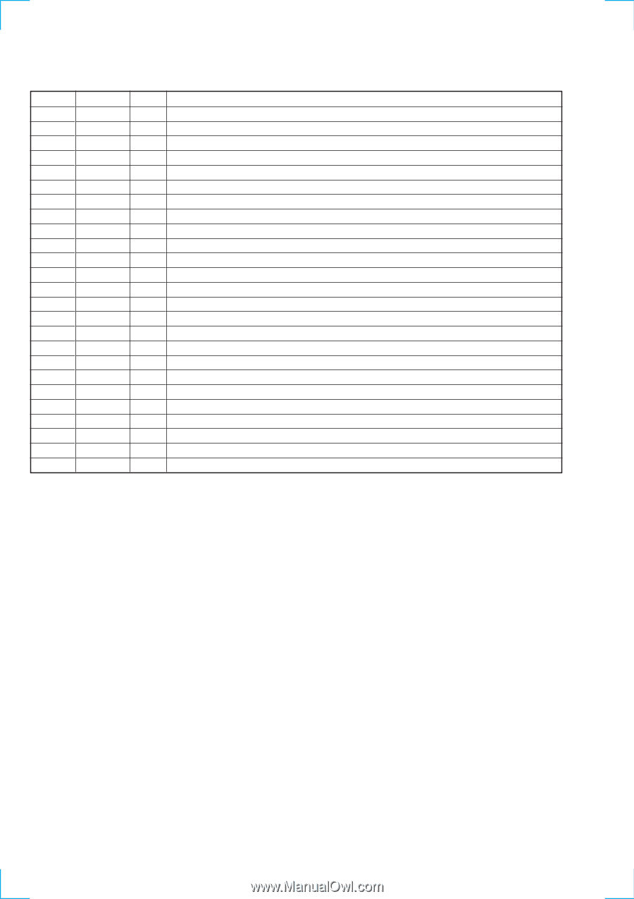
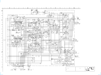
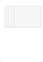
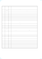
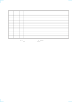
Pin No. Pin Name I/O 91 VSS0 - 92 - 94 EA13 - EA15 O 95 EA16 O 96 TSTA I 97 PLDIVF I 98 PLDIVB O 99 CLKI I 100 CLKO O 101 VSS1 - 102 VDD0 - 103 AVSS - 104 AVDD - 105 PLLCK I/O 106 XPLLEN I 107 TST I 108 LRCT I 109 LROUT O 110 BKOUT O 111 VSS2 - 112 VDD1 - 113 BCK0 I 114 BCK1 I 115 LRCK0 I 116 LRCK1 I 117 - 120 SIA - SID I Description Ground External RAM address output Not used Test data input "L" = normal "H" = test (Connecting to ground) PLL input frequency select "L" = 256Fs "H" = 128Fs (Connecting to ground) PLL output frequency select "L" = 768Fs "H" = 1024Fs (Connecting to ground) Master clock input Master clock output (Not used) Ground +3.3V Ground for PLL cell VDD for PLL cell PLL output/test clock input PLL cell oscillation enable "L" oscillation enable "H" oscillation stop (Connecting to ground) Test data input "L" = normal "H" = test (Connecting to ground) Frequency counter input (Connecting to ground) LRCK0 divider output BCK0 divider output Ground +3.3V BCK input BCK input LRCK input LRCK input Serial data input - 50 -
-
 1
1 -
2
-
3
-
4
-
5
-
6
-
7
-
8
-
9
-
10
-
11
-
12
-
13
-
14
-
15
-
16
-
17
-
18
-
19
-
20
-
21
-
22
-
 23
23 -
 24
24 -
 25
25 -
 26
26 -
 27
27 -
 28
28 -
 29
29 -
 30
30 -
 31
31 -
 32
32 -
 33
33 -
34
-
35
-
36
-
37
-
38
-
39
-
40
-
41
-
42
-
43
-
44
-
45
-
46
-
47
-
48
-
49
-
50
-
51
-
52
-
53
-
54
-
55
-
56
-
57
-
58
-
59
-
60
-
61
-
62
-
63
-
64
 |
 |