ASRock 4Core1333-Viiv User Manual - Page 56
Chipset Configuration, Chipset Configuration
 |
View all ASRock 4Core1333-Viiv manuals
Add to My Manuals
Save this manual to your list of manuals |
Page 56 highlights
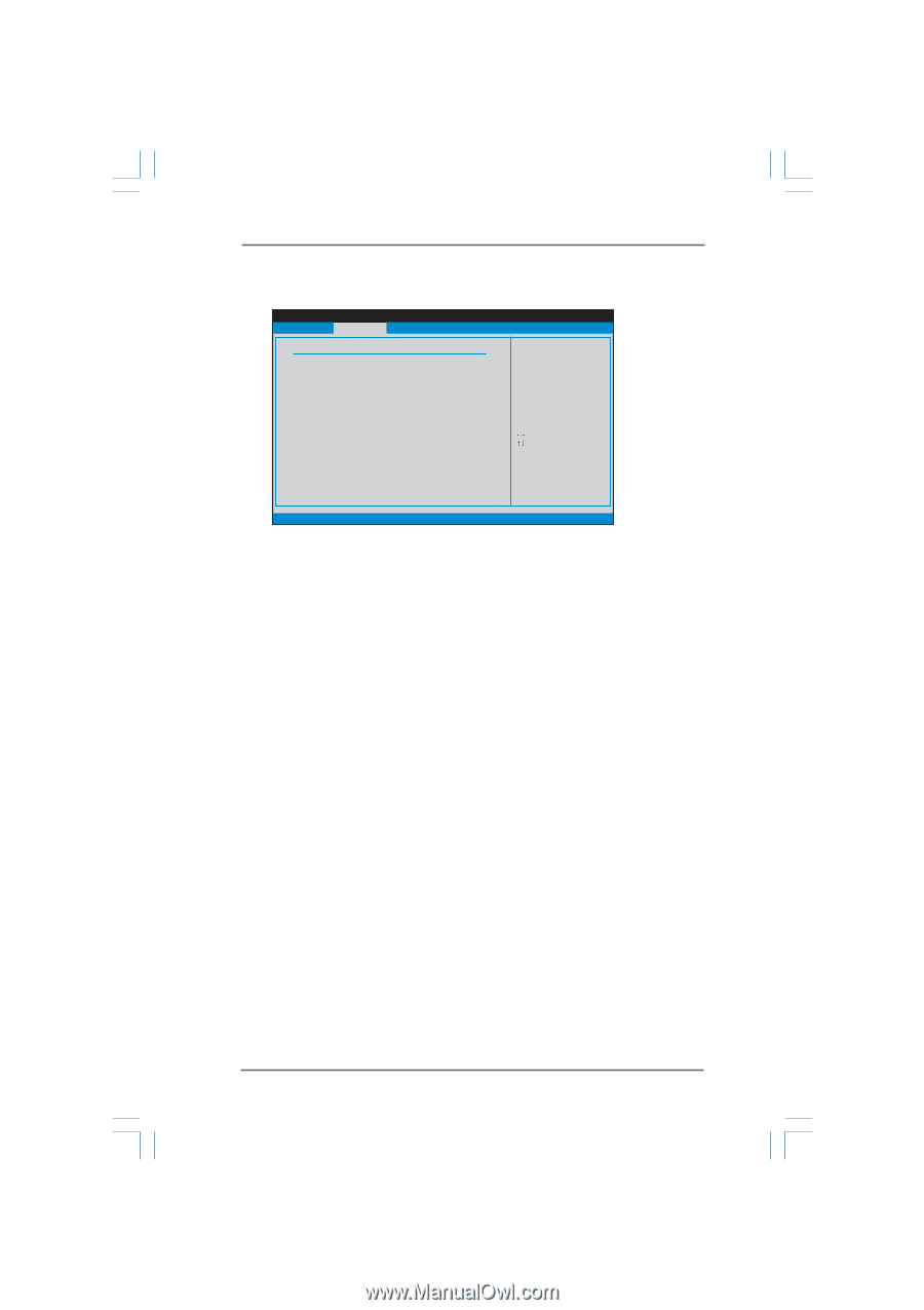
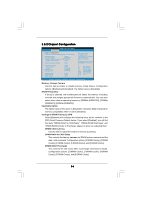
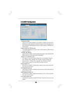
3.3.2 Chipset Configuration BIOS SETUP UTILITY Advanced Chipset Configuration Memory Remap Feature [Disabled] DRAM Frequency [Auto] Flexibility Option [Disabled] Configure DRAM Timing by SPD [Enabled] DRAM CAS# Latency [Auto] Primary Graphics Adapter [PCI] OnBoard HD Audio Front Panel CD-In OnBoard Lan OnBoard 1394 [Auto] [Auto] [Enabled] [Enabled] [Enabled] VCCM Voltage VDDQ Voltage ICH8 Voltage [Auto] [Low] [Low] ENABLE: Allow remapping of overlapped PCI memory above the total physical memory. DISABLE: Do not allow remapping of memory. +F1 F9 F10 ESC Select Screen Select Item Change Option General Help Load Defaults Save and Exit Exit v02.54 (C) Copyright 1985-2005, American Megatrends, Inc. Memory Remap Feature Use this item to enable or disable memory remap feature. Configuration options: [Enabled] and [Disabled]. The default value is [Disabled]. DRAM Frequency If [Auto] is selected, the motherboard will detect the memory module(s) inserted and assigns appropriate frequency automatically. You may also select other value as operating frequency: [266MHz (DDRII533)], [333MHz (DDRII667)], [400MHz (DDRII800)]. Flexibility Option The default value of this option is [Disabled]. It will allow better tolerance for memory compatibility when it is set to [Enabled]. Configure DRAM Timing by SPD Select [Enabled] will configure the following items by the contents in the SPD (Serial Presence Detect) device. If you select [Disabled], you will find the items "DRAM RAS# to CAS# Delay", "DRAM RAS# Precharge", and "DRAM RAS# Activate to Precharge" appear to allow you adjusting them. DRAM CAS# Latency Use this item to adjust the means of memory accessing. DRAM RAS# to CAS# Delay This controls the latency between the DRAM active command and the read / write command. Configuration options: [2 DRAM Clocks], [3 DRAM Clocks], [4 DRAM Clocks], [5 DRAM Clocks], and [6 DRAM Clocks]. DRAM RAS# Precharge This controls the idle clocks after a precharge command is issued. Configuration options: [2 DRAM Clocks], [3 DRAM Clocks], [4 DRAM Clocks], [5 DRAM Clocks], and [6 DRAM Clocks]. 56
-
 1
1 -
2
-
3
-
4
-
5
-
6
-
7
-
8
-
9
-
10
-
11
-
12
-
13
-
14
-
15
-
16
-
17
-
18
-
19
-
20
-
21
-
22
-
23
-
24
-
25
-
26
-
27
-
28
-
29
-
30
-
31
-
32
-
33
-
34
-
35
-
36
-
37
-
38
-
39
-
40
-
41
-
42
-
43
-
44
-
45
-
46
-
47
-
48
-
49
-
50
-
 51
51 -
 52
52 -
 53
53 -
 54
54 -
 55
55 -
 56
56 -
 57
57 -
 58
58 -
 59
59 -
 60
60 -
 61
61 -
62
-
63
-
64
-
65
-
66
-
67
-
68
 |
 |