Fujitsu MHN2100AT Manual/User Guide - Page 192
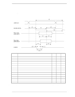
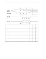
Table 5.19, Ultra DMA sender and recipient timing requirements
 |
View all Fujitsu MHN2100AT manuals
Add to My Manuals
Save this manual to your list of manuals |
Page 192 highlights
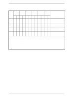
Interface Table 5.19 Ultra DMA sender and recipient timing requirements MODE 0 MODE 1 MODE 2 MODE 3 MODE 4 MODE 5 (in ns) (in ns) (in ns) (in ns) (in ns) (in ns) NAME MIN MAX MIN MAX MIN MAX MIN MAX MIN MAX MIN MAX COMMENT tDSIC 14.7 9.7 6.8 6.8 4.8 2.3 Recipient IC data setup time (from data valid until STROBE edge) (*1) tDHIC 4.8 4.8 4.8 4.8 4.8 2.8 Recipient IC data hold time (from STROBE edge until data may become invalid) (*1) tDVSIC 72.9 50.9 33.9 22.6 9.5 6 Sender IC data valid setup time (from data valid until STROBE edge) (*2) tDVHIC 9 9 9 9 9 6 Sender IC data valid hold time (from STROBE edge until data may become invalid) (*2) *1: The correct data value shall be captured by the recipient given input data with a slew rate of 0.4 V/ns rising and falling and the input STROBE with a slew rate of 0.4 V/ns rising and falling at tDSIC and tDHIC timing (as measured through 1.5V). *2: The parameters tDVSIC and tDVHIC shall be met for lumped capacitive loads of 15 and 40 pf at the IC where all signals have the same capacitive load value. Noise that may couple onto the output signals from external sources in a normally functioning system has not been included in these values. Note: All timing measurement switching points (low to high and high to low) shall be taken at 1.5V. 5-116 C141-E120-02EN
-
 1
1 -
2
-
3
-
4
-
5
-
6
-
7
-
8
-
9
-
10
-
11
-
12
-
13
-
14
-
15
-
16
-
17
-
18
-
19
-
20
-
21
-
22
-
23
-
24
-
25
-
26
-
27
-
28
-
29
-
30
-
31
-
32
-
33
-
34
-
35
-
36
-
37
-
38
-
39
-
40
-
41
-
42
-
43
-
44
-
45
-
46
-
47
-
48
-
49
-
50
-
51
-
52
-
53
-
54
-
55
-
56
-
57
-
58
-
59
-
60
-
61
-
62
-
63
-
64
-
65
-
66
-
67
-
68
-
69
-
70
-
71
-
72
-
73
-
74
-
75
-
76
-
77
-
78
-
79
-
80
-
81
-
82
-
83
-
84
-
85
-
86
-
87
-
88
-
89
-
90
-
91
-
92
-
93
-
94
-
95
-
96
-
97
-
98
-
99
-
100
-
101
-
102
-
103
-
104
-
105
-
106
-
107
-
108
-
109
-
110
-
111
-
112
-
113
-
114
-
115
-
116
-
117
-
118
-
119
-
120
-
121
-
122
-
123
-
124
-
125
-
126
-
127
-
128
-
129
-
130
-
131
-
132
-
133
-
134
-
135
-
136
-
137
-
138
-
139
-
140
-
141
-
142
-
143
-
144
-
145
-
146
-
147
-
148
-
149
-
150
-
151
-
152
-
153
-
154
-
155
-
156
-
157
-
158
-
159
-
160
-
161
-
162
-
163
-
164
-
165
-
166
-
167
-
168
-
169
-
170
-
171
-
172
-
173
-
174
-
175
-
176
-
177
-
178
-
179
-
180
-
181
-
182
-
183
-
184
-
185
-
186
-
 187
187 -
 188
188 -
 189
189 -
 190
190 -
 191
191 -
 192
192 -
 193
193 -
 194
194 -
 195
195 -
 196
196 -
 197
197 -
198
-
199
-
200
-
201
-
202
-
203
-
204
-
205
-
206
-
207
-
208
-
209
-
210
-
211
-
212
-
213
-
214
-
215
-
216
-
217
-
218
-
219
-
220
-
221
-
222
-
223
-
224
-
225
-
226
-
227
-
228
-
229
-
230
-
231
-
232
-
233
-
234
-
235
-
236
 |
 |
