Intel D845GVFN Product Specification - Page 13
Block Diagram - graphics drive
 |
View all Intel D845GVFN manuals
Add to My Manuals
Save this manual to your list of manuals |
Page 13 highlights
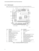
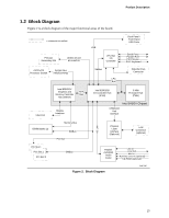
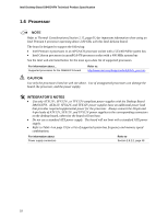
Product Description 1.2 Block Diagram Figure 2 is a block diagram of the major functional areas of the board. = connector or socket Primary/ Secondary IDE UDMA 33 and ATA-66/100 mPGA478 Processor Socket System Bus (400/533 MHz) USB LPC Bus I/O Controller SMBus LPC Bus Back Panel / Front Panel USB Ports Serial Ports Parallel Port PS/2 Mouse PS/2 Keyboard Diskette Drive Connector Intel 82845GV Graphics and Memory Controller Hub (GMCH) AHA Bus VGA Port DIMM Banks (2) Display Interface Memory Bus SMBus PCI Bus Intel 82801DB I/O Controller Hub (ICH4) 3 Mbit Firmware Hub (FWH) Intel 845GV Chipset CSMA/CD Unit Interface AC Link Physical Layer Interface (Optional) LAN Connector (optional) PCI Slot 1 PCI Slot 2 PCI Slot 3 SMBus Realtek ALC202A Audio Codec Figure 2. Block Diagram Line In Line Out Mic In Auxiliary Line In (optional) CD-ROM (optional) OM17285 13
-
 1
1 -
2
-
3
-
4
-
5
-
6
-
7
-
 8
8 -
 9
9 -
 10
10 -
 11
11 -
 12
12 -
 13
13 -
 14
14 -
 15
15 -
 16
16 -
 17
17 -
 18
18 -
19
-
20
-
21
-
22
-
23
-
24
-
25
-
26
-
27
-
28
-
29
-
30
-
31
-
32
-
33
-
34
-
35
-
36
-
37
-
38
-
39
-
40
-
41
-
42
-
43
-
44
-
45
-
46
-
47
-
48
-
49
-
50
-
51
-
52
-
53
-
54
-
55
-
56
-
57
-
58
-
59
-
60
-
61
-
62
-
63
-
64
-
65
-
66
-
67
-
68
-
69
-
70
-
71
-
72
-
73
-
74
-
75
-
76
-
77
-
78
-
79
-
80
-
81
-
82
-
83
-
84
 |
 |
