Intel DN2820FYK Technical Product Specification - Page 33
Technical Reference
 |
View all Intel DN2820FYK manuals
Add to My Manuals
Save this manual to your list of manuals |
Page 33 highlights
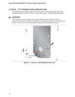
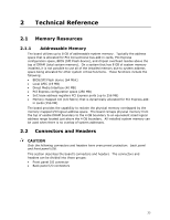
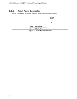
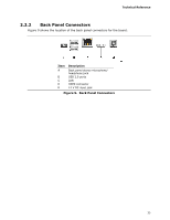
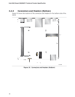
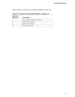
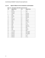
2 Technical Reference 2.1 Memory Resources 2.1.1 Addressable Memory The board utilizes up to 8 GB of addressable system memory. Typically the address space that is allocated for PCI Conventional bus add-in cards, PCI Express configuration space, BIOS (SPI Flash device), and chipset overhead resides above the top of DRAM (total system memory). On a system that has 8 GB of system memory installed, it is not possible to use all of the installed memory due to system address space being allocated for other system critical functions. These functions include the following: • BIOS/SPI Flash device (64 Mbit) • Local APIC (19 MB) • Direct Media Interface (40 MB) • PCI Express configuration space (256 MB) • SoC base address registers PCI Express ports (up to 256 MB) • Memory-mapped I/O (I/O fabric) that is dynamically allocated for PCI Express add- in cards (256 MB) The board provides the capability to reclaim the physical memory overlapped by the memory mapped I/O logical address space. The board remaps physical memory from the top of usable DRAM boundary to the 4 GB boundary to an equivalent sized logical address range located just above the 4 GB boundary. All installed system memory can be used when there is no overlap of system addresses. 2.2 Connectors and Headers CAUTION Only the following connectors and headers have overcurrent protection: back panel and front panel USB. This section describes the board's connectors and headers. The connectors and headers can be divided into these groups: • Front panel I/O connector • Back panel I/O connectors 33
-
 1
1 -
2
-
3
-
4
-
5
-
6
-
7
-
8
-
9
-
10
-
11
-
12
-
13
-
14
-
15
-
16
-
17
-
18
-
19
-
20
-
21
-
22
-
23
-
24
-
25
-
26
-
27
-
 28
28 -
 29
29 -
 30
30 -
 31
31 -
 32
32 -
 33
33 -
 34
34 -
 35
35 -
 36
36 -
 37
37 -
 38
38 -
39
-
40
-
41
-
42
-
43
-
44
-
45
-
46
-
47
-
48
-
49
-
50
-
51
-
52
-
53
-
54
-
55
-
56
-
57
-
58
-
59
-
60
-
61
-
62
-
63
-
64
-
65
-
66
-
67
-
68
 |
 |