Seagate ST800FM0022 Pulsar.2 SAS Product Manual - Page 63
SAS transmitters and receivers, Power, Ready LED Out
 |
View all Seagate ST800FM0022 manuals
Add to My Manuals
Save this manual to your list of manuals |
Page 63 highlights
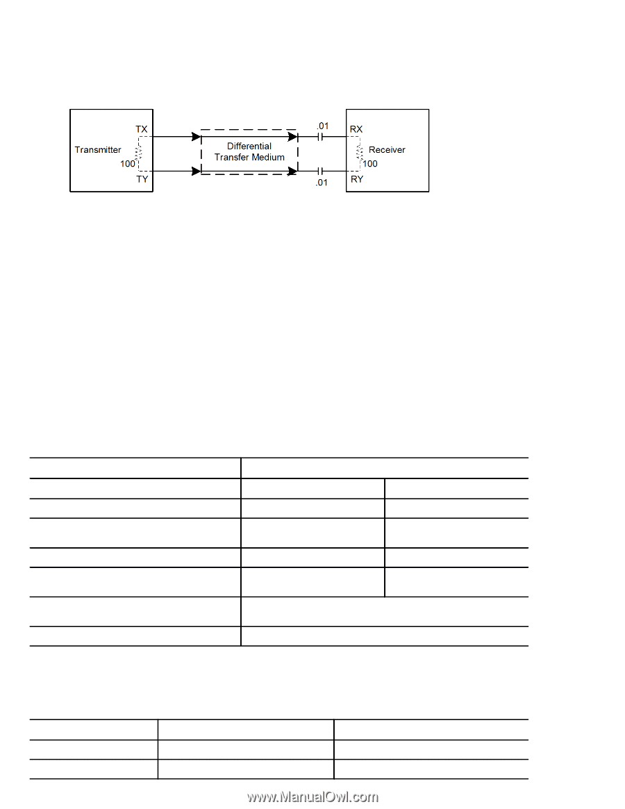
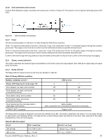
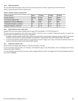
11.4.6 SAS transmitters and receivers A typical SAS differential copper transmitter and receiver pair is shown in Figure 20. The receiver is AC coupling to eliminate ground shift noise. Figure 20. SAS transmitters and receivers 11.4.7 Power The drive receives power (+5 volts and +12 volts) through the SAS device connector. Three +12 volt pins provide power to the drive, 2 short and 1 long. The current return for the +12 volt power supply is through the common ground pins. The supply current and return current must be distributed as evenly as possible among the pins. Three +5 volt pins provide power to the drive, 2 short and 1 long. The current return for the +5 volt power supply is through the common ground pins. The supply current and return current must be distributed as evenly as possible among the pins. Current to the drive through the long power pins may be limited by the system to reduce inrush current to the drive during hot plugging. 11.5 SIGNAL CHARACTERISTICS This section describes the electrical signal characteristics of the drive's input and output signals. See Table 24 for signal type and signal name information. 11.5.1 Ready LED Out The Ready LED Out signal is driven by the drive as indicated in Table 25. Table 25 Ready LED Out conditions NORMAL COMMAND ACTIVITY LED STATUS Ready LED Meaning bit mode page 19h 0 1 Drive stopped, not ready, and no activity Drive stopped, not ready, and activity (command executing) Drive started, ready, and no activity Drive started, ready, and activity (command executing) Drive transitioning from not-ready state to ready state or the reverse. FORMAT UNIT in progress, Off Off On On On Off Off On Blinks steadily (50% on and 50% off, 0.5 seconds on and off for 0.5 seconds) Toggles on/off The Ready LED Out signal is designed to pull down the cathode of an LED. The anode is attached to the proper +3.3 volt supply through an appropriate current limiting resistor. The LED and the current limiting resistor are external to the drive. See Table 26 for the output characteristics of the LED drive signals. Table 26 LED drive signal STATE TEST CONDITION OUTPUT VOLTAGE LED off, high LED on, low 0 V ≤ VOH ≤ 3.6 V IOL = 15 mA -100 μA < IOH < 100 μA 0 ≤ VOL ≤ 0.225 V PULSAR.2 SAS PRODUCT MANUAL, REV. C 57
-
 1
1 -
2
-
3
-
4
-
5
-
6
-
7
-
8
-
9
-
10
-
11
-
12
-
13
-
14
-
15
-
16
-
17
-
18
-
19
-
20
-
21
-
22
-
23
-
24
-
25
-
26
-
27
-
28
-
29
-
30
-
31
-
32
-
33
-
34
-
35
-
36
-
37
-
38
-
39
-
40
-
41
-
42
-
43
-
44
-
45
-
46
-
47
-
48
-
49
-
50
-
51
-
52
-
53
-
54
-
55
-
56
-
57
-
 58
58 -
 59
59 -
 60
60 -
 61
61 -
 62
62 -
 63
63 -
 64
64 -
 65
65 -
 66
66 -
 67
67 -
 68
68 -
69
 |
 |