Sharp XE-A202 Service Manual - Page 12
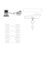
Rs232 Circuit
 |
UPC - 074000048270
View all Sharp XE-A202 manuals
Add to My Manuals
Save this manual to your list of manuals |
Page 12 highlights
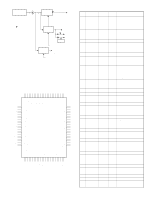
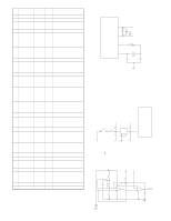
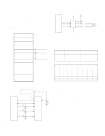
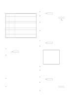
1) Keyboard Scan signal: 10 /S0-9 signals Return signal: 6 P92-97 signals The keys are read by the key matrix following the above signals. 2) Mode switch Scan signal: 8 /S0-7 signals Return signal: 1 P90 signal The positions are read by the above signals. Scan signal /S0 /S1 /S2 /S3 /S4 /S5 /S6 /S7 Mode switch SRV PGM (OFF) TIME REG MGR X1/Z1 X2/Z2 position 3) Paper feed key Scan signal: 1 /S1 signal Return signal: 1 P91 signal The paper feed key is read by the above signals. 4) Head up sensor Scan signal: 1 /S3 signal Return signal: 1 P91 signal The Head up sensor state is read by the above signals. Head up sensor Head up detected Head up not detected P91 Low High 5) Paper end sensor Scan signal: 1 /S4 signal Return signal: 1 P91 signal The paper end sensor state is read by the above signals. Receipt near end sensor P91 End detected Low End not detected High 6) RS232/CI signal detection Scan signal: 1 /S9 signal Return signal: 1 P91 signal The RS232/CI signal is detected by the above signals. RS232 /CI signal /CI signal detected P91 Low /CI signal not detected High 7) Display Scan signal: 10 /S0-9 signals The above 10 scan signals are used as the following digit signals. Digit signal: Scan signal /S0 /S1 /S2 /S3 /S4 /S5 /S6 /S7 /S8 /S9 Digit signal: G1' G2' G3' G4' G5' G6' G7' G8' G9' G10 Front ' Digit signal: G1' G2' G3' G4' G5' G6' G7' Pop-up Segment signal : Segment signals: a, b, c, d, e, f, g, and DP are output by the IC:74HC374, using the data bus signal:D0-7 from the CPU as an input signal and the chip select signal:/CS3 as a latch signal. 12. RS232 CIRCUIT CPU P75 P66 P67 P74 P77 P64 P76 P91 R2OUT R2IN R1OUT R1IN T3IN T3OUT T2IN T2OUT HIN211 R4OUT R4IN T1IN T1OUT R5OUT R5IN R3OUT R3IN CD RD SD ER DR RS CS CI /S9 Q14 D16 IC14 The signals from the CPU are converted by the HIN211 into the RS232 level to input and output them. 1 CD 2 RD 3 SD 4 ER 5 GND 6 DR 7 RS 8 CS 9 CI D-SUB 9pin connector XE-A202U HARDWARE DESCRIPTION - 11 -
-
 1
1 -
2
-
3
-
4
-
5
-
6
-
 7
7 -
 8
8 -
 9
9 -
 10
10 -
 11
11 -
 12
12 -
 13
13 -
 14
14 -
 15
15 -
 16
16 -
 17
17 -
18
-
19
-
20
-
21
-
22
-
23
-
24
-
25
-
26
-
27
 |
 |