Sharp XE-A202 Service Manual - Page 9
Clock Generator, Reset Circuit, P-off Circuit - supplies
 |
UPC - 074000048270
View all Sharp XE-A202 manuals
Add to My Manuals
Save this manual to your list of manuals |
Page 9 highlights
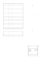
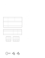
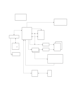
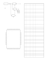
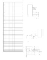
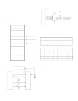
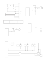
Pin No. SYMBOL 53 A17 54 A16 55 A15 56 A14 57 A13 58 A12 59 A11 60 A10 61 A9 62 VCC 63 A8 64 VSS 65 A7 66 A6 67 A5 68 A4 69 A3 70 A2 71 A1 72 A0 73 P17 74 P16 75 P15 76 P14 77 P13 78 P12 79 P11 80 P10 81 D7 82 D6 83 D5 84 D4 85 D3 86 D2 87 D1 88 D0 89 AN7 90 AN6 91 AN5 92 AN4 93 AN3 94 AN2 95 AN1 96 AVSS 97 AN0 98 VREF 99 AVCC 100 SIN4 SIGNAL NAME A17 A16 A15 A14 A13 A12 A11 A10 A9 VDD A8 VSS A7 A6 A5 A4 A3 A2 A1 A0 ENA2 ENA1 IN2 IN1 P13 P12 P11 P10 D7 D6 D5 D4 D3 D2 D1 D0 STB1 LATCH P105 P104 P103 Vref P101 VSS TH VDD VDD P97 In/ Out Out Out Out Out Out Out Out Out Out In Out In Out Out Out Out Out Out Out Out Out Out Out Out Out Out Out Out InOut InOut InOut InOut InOut InOut InOut InOut Out Out Out Out In In In In In In In In Function Address bus :17 Address bus :16 Address bus :15 Address bus :14 Address bus :13 Address bus :12 Address bus :11 Address bus :10 Address bus :9 VDD Address bus :8 VSS Address bus :7 Address bus :6 Address bus :5 Address bus :4 Address bus :3 Address bus :2 Address bus :1 Address bus :0 Paper feed motor :ENA2 Paper feed motor :ENA1 Paper feed motor :IN2 Paper feed motor :IN1 Key/Display Key/Display Key/Display Key/Display Data bus :7 Data bus :6 Data bus :5 Data bus :4 Data bus :3 Data bus :2 Data bus :1 Data bus :0 Printer head strobe Printer data latch Printer head voltage ON CG ROM Bank VBAT NU Vret Printer head voltage check VSS Print head temperature check VDD VDD Key IN 3. CLOCK GENERATOR 1) CPU 15 XIN CPU 13 XOUT 12MHz R 11 330 XCOUT 10 XCIN X1 32.768KHz C C 18P 27P Two oscillators are connected to the CPU. The basic clock X2 is supplied from a 12MHz oscillator. If the CPU was not operating properly, the signal does not appear on this line in most cases. The sub-clock X1 generates 32.768KHz which is primarily used to update the internal RTC (real time clock). During the standby mode, it keeps oscillating to update the clock and monitoring the power recovery. 4. RESET CIRCUIT MODE SWITCH SRV' position VDD VDD IC R S-80928ANMP R R C C CPU 11 /RESET (1) When the mode switch is placed in the "SRV" position, the reset signal is sent to the CPU to reset the hardware. (2) When VDD t 2.8V, a reset signal is outputted from the reset IC. (S80928ANMP) 5. P-OFF CIRCUIT VCC VLED R15 2.7K C14 1uF/50V R16 9.1KG R19 R17 56K 0 8 3 1 2 IC4A 4 R18 BA10393 3.9K R20 2.7K 5 8 6 4 IC4B BA10393 7 /POFF C15 0.1uF ZD4 MTZJ5.1B P-OFF XE-A202U HARDWARE DESCRIPTION - 8 -
-
 1
1 -
2
-
3
-
 4
4 -
 5
5 -
 6
6 -
 7
7 -
 8
8 -
 9
9 -
 10
10 -
 11
11 -
 12
12 -
 13
13 -
 14
14 -
15
-
16
-
17
-
18
-
19
-
20
-
21
-
22
-
23
-
24
-
25
-
26
-
27
 |
 |
